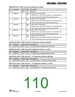
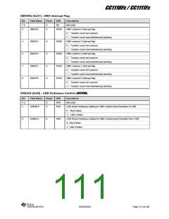
CC1110Fx / CC1111Fx
12.6.4
Input Capture Mode
output pins are glitch-free when operating in a
given output compare mode. Writing to the
compare register T1CCnL is buffered so that a
value written to T1CCnL does not take effect
until the corresponding high order register,
T1CCnH is written. For output compare modes
0 - 2, a new value written to the compare
register T1CCnH:T1CCnL takes effect after
the registers have been written. For other
output compare modes the new value written
to the compare register takes effect when the
timer reaches 0x0000.
When a channel is configured as an input
capture channel, the I/O pin associated with
that channel, is configured as an input. After
the timer has been started, a rising edge,
falling edge or any edge on the input pin will
trigger a capture of the 16-bit counter contents
into the associated capture register. Thus the
timer is able to capture the time when an
external event takes place.
The channel input pin is synchronized to the
internal system clock. Thus pulses on the input
pin must have a minimum duration greater
than the system clock period.
Note that channel 0 has fewer output compare
modes than channel
1 and 2 because
T1CC0H:T1CC0L has a special function in
modes 5 and 6, meaning these modes would
not be useful for channel 0.
The contents of the 16-bit capture register can
be read from registers T1CCnH:T1CCnL.
When the capture takes place, the interrupt
When a compare occurs, the interrupt flag for
the appropriate channel (T1CTL.CH0IF,
T1CTL.CH1IF, or T1CTL.CH2IF for channel
0, 1, and 2 respectively) is asserted. The
IRCON.T1IF flag is only asserted if the
corresponding interrupt mask bit T1CCTL0.IM,
T1CCTL1.IM, or T1CCTL2.IM is set to 1. An
interrupt request is generated if the
corresponding interrupt mask bit is set together
with IEN1.T1EN. When operating in up-down
mode, the interrupt flag for channel 0 is set
when the counter reaches 0x0000 instead of
when a compare occurs.
flag
for
the
appropriate
channel
(T1CTL.CH0IF,
T1CTL.CH1IF,
or
T1CTL.CH2IF for channel 0, 1, and 2
respectively) is asserted. The IRCON.T1IF
flag is only asserted if the corresponding
interrupt mask bit T1CCTL0.IM, T1CCTL1.IM,
or T1CCTL2.IM is set to 1. An interrupt
request is generated if the corresponding
interrupt mask bit is set together with
IEN1.T1EN.
12.6.4.1 RF Event Capture
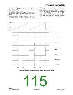
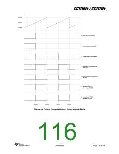
Examples of output compare modes in various
timer modes are given in Figure 32, Figure 33,
and Figure 34.
Each timer channel may be configured so that
the RF events associated with the RF interrupt
(interrupt #16) will trigger a capture instead of
the normal input pin capture. This is done by
Edge-aligned: PWM output signals can be
generated using the timer modulo mode and
channels 1 and 2 in output compare mode 5 or
6 (defined by T1CCTLn.CMPbits, where nis 1
or 2) as shown in Figure 33. The period of the
PWM signal is determined by the setting in
T1CC0 and the duty cycle is determined by
T1CCn.
setting
T1CCTLn.CPSEL=1. When
this
configuration is chosen, the RF event(s)
enabled by RFIM (see Section 13.3.1 on Page
188) will trigger a capture. This way the timer
can be used to capture a value when e.g. a
start of frame delimiter (SFD) is detected.
Note: When using an RF event to trigger a
capture, both CLKCON.CLKSPDand
CLKCON.TICKSPDmust be set to 000.
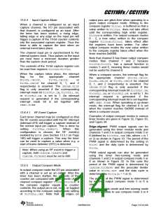
PWM output signals can also be generated
using the timer free-running mode and
channels 1 and 2 in output compare mode 5 or
6 as shown in Figure 32. In this case the
period of the PWM signal is determined by
CLKCON.TICKSPD and the prescaler divider
value in T1CTL.DIV and the duty cycle is
determined by T1CCn(n= 1 or 2).
12.6.5
Output Compare Mode
In output compare mode the I/O pin associated
with a channel is set as an output. After the
timer has been started, the contents of the
counter are compared with the contents of the
channel compare register T1CCnH:T1CCnL. If
the compare register equals the counter
contents, the output pin is set, reset, or toggled
according to the compare output mode setting
of T1CCTLn.CMP. Note that all edges on
The polarity of the PWM signal is determined
by whether output compare mode 5 or 6 is
used.
For both modulo mode and free-running mode
it is also possible to use compare mode 3 or 4
SWRS033H
Page 114 of 246

 TI [ TEXAS INSTRUMENTS ]