CC1110Fx / CC1111Fx
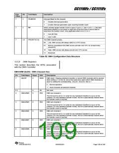
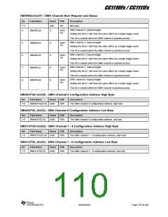
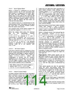
DMAREQ (0xD7) - DMA Channel Start Request and Status
Bit
7:5
4
Field Name
Reset
000
0
R/W
Description
R0
Not used
DMA channel 4, manual trigger
DMAREQ4
R/W1
H0
Setting this bit to 1 will have the same effect as a single trigger event.
This bit is cleared when the DMA channel is granted access.
DMA channel 3, manual trigger
3
2
1
0
DMAREQ3
DMAREQ2
DMAREQ1
DMAREQ0
0
0
0
0
R/W1
H0
Setting this bit to 1 will have the same effect as a single trigger event.
This bit is cleared when the DMA channel is granted access.
DMA channel 2, manual trigger
R/W1
H0
Setting this bit to 1 will have the same effect as a single trigger event.
This bit is cleared when the DMA channel is granted access.
DMA channel 1, manual trigger
R/W1
H0
Setting this bit to 1 will have the same effect as a single trigger event.
This bit is cleared when the DMA channel is granted access.
DMA channel 0, manual trigger
R/W1
H0
Setting this bit to 1 will have the same effect as a single trigger event.
This bit is cleared when the DMA channel is granted access.
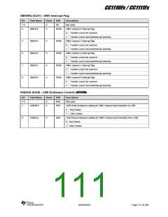
DMA0CFGH (0xD5) - DMA Channel 0 Configuration Address High Byte
Bit
Field Name
Reset
R/W
Description
7:0
DMA0CFG[15:8] 0x00
R/W
The DMA channel 0 configuration address, high byte
DMA0CFGL (0xD4) - DMA Channel 0 Configuration Address Low Byte
Bit
Field Name
Reset
R/W
Description
7:0
DMA0CFG[7:0]
0x00
R/W
The DMA channel 0 configuration address, low byte
DMA1CFGH (0xD3) - DMA Channel 1 - 4 Configuration Address High Byte
Bit
Field Name
Reset
R/W
Description
7:0
DMA1CFG[15:8] 0x00
R/W
The DMA channel 1 - 4 configuration address, high byte
DMA1CFGL (0xD2) - DMA Channel 1 - 4 Configuration Address Low Byte
Bit
Field Name
Reset
R/W
Description
7:0
DMA1CFG[7:0]
0x00
R/W
The DMA channel 1 - 4 configuration address, low byte
SWRS033H
Page 110 of 246

 TI [ TEXAS INSTRUMENTS ]