CC1110Fx / CC1111Fx
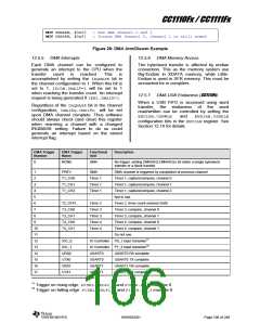
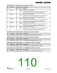
MOV DMAARM, #0x03
MOV DMAARM, #0x81
; Arm DMA channel 0 and 1
; Disarm DMA channel 0, channel 1 is still armed
Figure 28: DMA Arm/Disarm Example
12.5.5
DMA Interrupts
12.5.6
DMA Memory Access
Each DMA channel can be configured to
generate an interrupt to the CPU when the
The byte/word transfer is affected by endian
convention. This as the memory system use
Big-Endian in XDATA memory, while Little-
Endian is used in SFR memory. This must be
accounted for in compilers.
transfer
count
is
reached.
This
is
accomplished by setting the IRQMASK bit in
the channel configuration to 1. When this bit is
set to 1, IRCON.DMAIF=1 will be set to 1
when reaching the transfer count. An interrupt
request is being generated if IEN1.DMAIE=1.
12.5.7
DMA USB Endianess (CC1111Fx)
When a USB FIFO is accessed using word
transfer, the endianess of the word
read/written can be controlled by setting the
Regardless of the IRQMASK bit in the channel
configuration, DMAIRQ.DMAIFn will be set
upon DMA channel complete. Thus software
should always check (and clear) this register
when rearming a channel with a changed
IRQMASK setting. Failure to do so could
generate an interrupt based on the stored
interrupt flag.
ENDIAN.USBWLE
and
ENDIAN.USBRLE
configuration bits in the ENDIAN register. See
Section 12.16 for details.
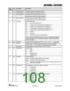
DMA Trigger
Number
DMA Trigger
Name
Functional
Unit
Description
0
NONE
DMA
No trigger, setting DMAREQ.DMAREQx bit starts a single byte/word
transfer or a block transfer
1
PREV
DMA
DMA channel is triggered by completion of previous channel
Timer 1, capture/compare, channel 0
Timer 1, capture/compare, channel 1
Timer 1, capture/compare, channel 2
Not in use.
2
T1_CH0
T1_CH1
T1_CH2
Timer 1
Timer 1
Timer 1
3
4
5
6
T2_OVFL
T3_CH0
T3_CH1
T4_CH0
T4_CH1
Timer 2
Timer 3
Timer 3
Timer 4
Timer 4
Timer 2, timer count reaches 0x00
Timer 3, compare, channel 0
Timer 3, compare, channel 1
Timer 4, compare, channel 0
Timer 4, compare, channel 1
Do not use
7
8
9
10
11
12
13
14
15
16
17
IOC_0
IOC_1
URX0
UTX0
URX1
UTX1
IO Controller P0_1 input transition17
IO Controller P1_3 input transition18
USART0
USART0
USART1
USART1
USART0 RX complete
USART0 TX complete
USART1 RX complete
USART1 TX complete
17 Trigger on rising edge. P0SEL.SELP0_1and P0DIR.P0_1must be 0
18 Trigger on falling edge. P1SEL.SELP1_3and P1DIR.P1_3must be 0
SWRS033H
Page 106 of 246

 TI [ TEXAS INSTRUMENTS ]