bq51050B
bq51051B
www.ti.com
SLUSB42C –JULY 2012–REVISED FEBRUARY 2013
Status Outputs
The bq5105x provides one status output, CHG. This output is an open-drain NMOS device that is rated to 20 V.
The open-drain FET connected to the CHG pin will be turned on whenever the output (BAT) of the chagrer is
enabled. As a note, the output of the charger supply will not be enabled if the VRECT(REG) does not converge at
the no-load target voltage.
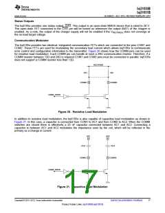
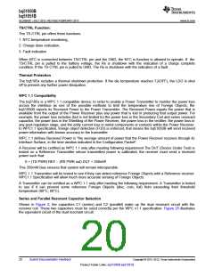
Communication Modulator
The bq5105x provides two identical, integrated communication FETs which are connected to the pins COM1 and
COM2. These FETs are used for modulating the secondary load current which allows bq5105x to communicate
error control and configuration information to the transmitter. Figure 20 shows how the COMM pins can be used
for resistive load modulation. Each COMM pin can handle at most a 24Ω communication resistor. Therefore, if a
COMM resistor between 12Ω and 24Ω is required COM1 and COM2 pins must be connected in parallel. bq5105x
does not support a COMM resistor less than 12Ω.
Figure 20. Resistive Load Modulation
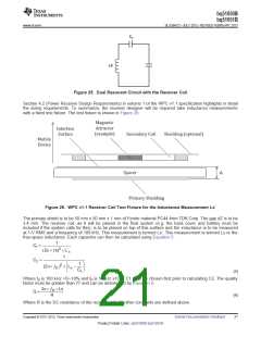
In addition to resistive load modulation, the bq5105x is also capable of capacitive load modulation as shown in
Figure 21. In this case, a capacitor is connected from COM1 to AC1 and from COM2 to AC2. When the COMM
switches are closed there is effectively a 22 nF capacitor connected between AC1 and AC2. Connecting a
capacitor in between AC1 and AC2 modulates the impedance seen by the coil, which will be reflected in the
primary as a change in current.
Figure 21. Capacitive Load Modulation
Copyright © 2012–2013, Texas Instruments Incorporated
Submit Documentation Feedback
17
Product Folder Links: bq51050B bq51051B

 TI [ TEXAS INSTRUMENTS ]