bq24707
bq24707A
www.ti.com
PIN
SLUSA78B –JULY 2010–REVISED MARCH 2011
PIN FUNCTIONS – 20-PIN QFN (continued)
DESCRIPTION
NO.
NAME
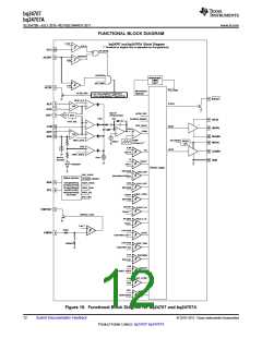
Charge current sense resistor positive input. Connect SRP pin to a 10 Ω resistor first then from resistor another
terminal connect to current sensing resistor. Connect a 0.1µF ceramic capacitor between current sensing resistor to
provide differential mode filtering. See application information about negative output voltage protection for hard shorts
on battery to ground or battery reverse connection by adding small resistor.
13
SRP
IC ground. On PCB layout, connect to the analog ground plane, and only connect to power ground plane through the
PowerPAD underneath the IC.
14
15
GND
LODRV
Low side power MOSFET driver output. Connect to low side n-channel MOSFET gate.
Linear regulator output. REGN is the output of the 6V linear regulator supplied from VCC. The LDO is active when the
voltage on the ACDET pin is above 0.6V and voltage on VCC is above UVLO. Connect a 1uF ceramic capacitor from
REGN to GND.
16
REGN
High side power MOSFET driver power supply. Connect a 0.047µF capacitor from BTST to PHASE, and a bootstrap
Schottky diode from REGN to BTST.
17
BTST
18
19
HIDRV
PHASE
High side power MOSFET driver output. Connect to the high side n-channel MOSFET gate.
High side power MOSFET driver source. Connect to the source of the high side n-channel MOSFET.
Input supply, diode OR from adapter or battery voltage. Use 10Ω resistor and 1µF capacitor to ground as low pass
filter to limit inrush current.
20
VCC
Exposed pad beneath the IC. Analog ground and power ground star-connected only at the PowerPAD plane. Always
solder PowerPAD to the board, and have vias on the PowerPAD plane connecting to analog ground and power
ground planes. It also serves as a thermal pad to dissipate the heat.
PowerPAD
© 2010–2011, Texas Instruments Incorporated
Submit Documentation Feedback
11
Product Folder Link(s): bq24707 bq24707A

 TI [ TEXAS INSTRUMENTS ]