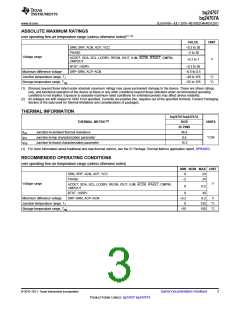
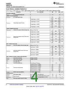
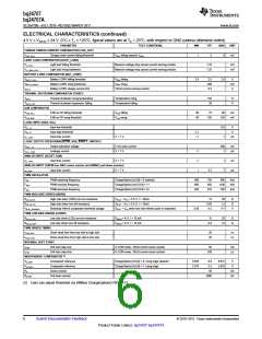
bq24707
bq24707A
www.ti.com
SLUSA78B –JULY 2010–REVISED MARCH 2011
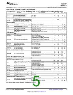
ELECTRICAL CHARACTERISTICS (continued)
4.5 V ≤ V(VCC) ≤ 24 V, 0°C ≤ TJ ≤ 125°C, typical values are at TA = 25°C, with respect to GND (unless otherwise noted)
PARAMETER
TEST CONDITIONS
MIN
TYP
MAX
UNIT
SMBus TIMING CHARACTERISTICS
tR
SCLK/SDATA rise time
SCLK/SDATA fall time
SCLK pulse width high
SCLK pulse width low
1
300
50
μs
ns
μs
μs
μs
tF
tW(H)
tW(L)
tSU(STA)
4
4.7
4.7
Setup time for START condition
START condition hold time after which first clock
pulse is generated
tH(STA)
4
μs
tSU(DAT)
tH(DAT)
tSU(STOP)
t(BUF)
Data setup time
250
300
4
ns
ns
Data hold time
Setup time for STOP condition
Bus free time between START and STOP condition
Clock frequency
µs
4.7
10
μs
FS(CL)
100
35
kHz
HOST COMMUNICATION FAILURE
ttimeout
SMBus bus release timeout(3)
tBOOT
25
10
ms
ms
Deglitch for watchdog reset signal
Watchdog timeout period, ChargeOption()
bit [14:13] = 01(4)
tWDI
tWDI
tWDI
35
70
44
88
53
105
210
s
s
s
Watchdog timeout period, ChargeOption()
bit [14:13] = 10(4)
Watchdog timeout period, ChargeOption()
bit [14:13] = 11(4) (default)
140
175
(3) Devices participating in a transfer timeout when any clock low exceeds the 25ms minimum timeout period. Devices that have detected a
timeout condition must reset the communication no later than the 35ms maximum timeout period. Both a master and a slave must
adhere to the maximum value specified as it incorporates the cumulative stretch limit for both a master (10ms) and a slave (25ms).
(4) User can adjust threshold via SMBus ChargeOption() REG0x12.
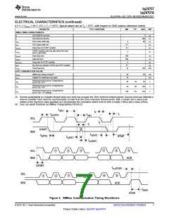
Figure 2. SMBus Communication Timing Waveforms
© 2010–2011, Texas Instruments Incorporated
Submit Documentation Feedback
7
Product Folder Link(s): bq24707 bq24707A

 TI [ TEXAS INSTRUMENTS ]