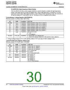
bq24160, bq24161
bq24163, bq24168
SLUSAO0A –NOVEMBER 2011–REVISED MARCH 2012
www.ti.com
The data transfer protocol for standard and fast modes is exactly the same; therefore, they are referred to as the
F/S-mode in this document. The bq2416x devices only support 7-bit addressing. The device 7-bit address is
defined as ‘1101011’ (6Bh).
F/S Mode Protocol
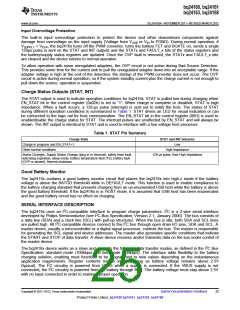
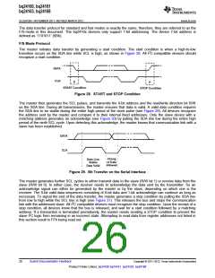
The master initiates data transfer by generating a start condition. The start condition is when a high-to-low
transition occurs on the SDA line while SCL is high, as shown in Figure 28. All I2C-compatible devices should
recognize a start condition.
DATA
CLK
S
P
START Condition
STOP Condition
Figure 28. START and STOP Condition
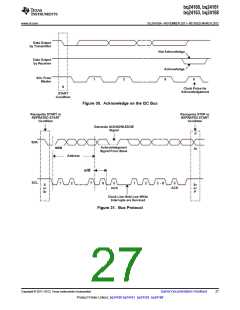
The master then generates the SCL pulses, and transmits the 8-bit address and the read/write direction bit R/W
on the SDA line. During all transmissions, the master ensures that data is valid. A valid data condition requires
the SDA line to be stable during the entire high period of the clock pulse (see Figure 29). All devices recognize
the address sent by the master and compare it to their internal fixed addresses. Only the slave device with a
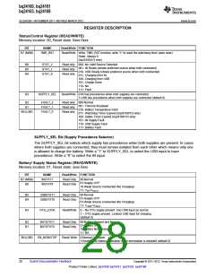
matching address generates an acknowledge (see Figure 30) by pulling the SDA line low during the entire high
period of the ninth SCL cycle. Upon detecting this acknowledge, the master knows that communication link with a
slave has been established.
DATA
CLK
Chang
of Data
Allowed
Data Line
Stable
Data Valid
Figure 29. Bit Transfer on the Serial Interface
The master generates further SCL cycles to either transmit data to the slave (R/W bit 1) or receive data from the
slave (R/W bit 0). In either case, the receiver needs to acknowledge the data sent by the transmitter. So an
acknowledge signal can either be generated by the master or by the slave, depending on which one is the
receiver. The 9-bit valid data sequences consisting of 8-bit data and 1-bit acknowledge can continue as long as
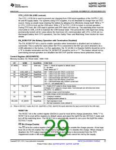
necessary. To signal the end of the data transfer, the master generates a stop condition by pulling the SDA line
from low to high while the SCL line is high (see Figure 31). This releases the bus and stops the communication
link with the addressed slave. All I2C compatible devices must recognize the stop condition. Upon the receipt of a
stop condition, all devices know that the bus is released, and wait for a start condition followed by a matching
address. If a transaction is terminated prematurely, the master needs sending a STOP condition to prevent the
slave I2C logic from remaining in an incorrect state. Attempting to read data from register addresses not listed in
this section result in FFh being read out.
26
Submit Documentation Feedback
Copyright © 2011–2012, Texas Instruments Incorporated
Product Folder Link(s): bq24160 bq24161 bq24163 bq24168

 TI [ TEXAS INSTRUMENTS ]