AM6548, AM6528, AM6526
ZHCSLA7B –DECEMBER 2019 –REVISED JUNE 2021
www.ti.com.cn
7.9 Timing and Switching Characteristics
Note
The Timing Requirements and Switching Characteristics values may change following the silicon
characterization result.
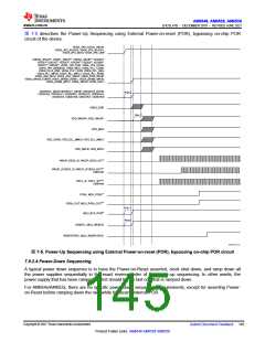
Note
The default SLEWRATE settings in each pad configuration register must be used to ensure timings,
unless specific instructions are given otherwise.
7.9.1 Timing Parameters and Information
The timing parameter symbols used in 节 7.9 are created in accordance with JEDEC Standard 100. To shorten
the symbols, some pin names and other related terminologies have been abbreviated in 表7-5:
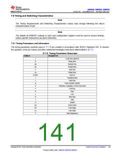
表7-5. Timing Parameters Subscripts
SYMBOL
PARAMETER
c
d
Cycle time (period)
Delay time
dis
en
h
Disable time
Enable time
Hold time
su
START
t
Setup time
Start bit
Transition time
Valid time
v
w
Pulse duration (width)
Unknown, changing, or don't care level
Fall time
X
F
H
High
L
Low
R
Rise time
V
Valid
IV
AE
FE
LE
Z
Invalid
Active Edge
First Edge
Last Edge
High impedance
Copyright © 2021 Texas Instruments Incorporated
Submit Document Feedback 141
Product Folder Links: AM6548 AM6528 AM6526

 TI [ TEXAS INSTRUMENTS ]