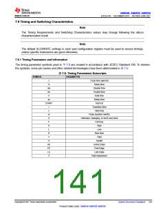
AM6548, AM6528, AM6526
ZHCSLA7B –DECEMBER 2019 –REVISED JUNE 2021
www.ti.com.cn
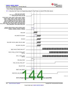
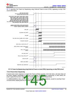
图 7-5 describes the Power-Up Sequencing using External Power-on-reset (POR), bypassing on-chip POR
circuit of the device.
VDDA_3P3_IOLDO_WKUP,
VDDA_3P3_IOLDO0, VDDA_3P3_IOLDO1,
VDDA_3P3_SDIO, VDDA_3P3_USB
VDDS0_WKUP(2), VDDS1_WKUP(2), VDDS2_WKUP(2), VDDS0(2)
VDDS1(2),VDDS2(2), VDDS3(2), VDDS4(2), VDDS5(2), VDDS6(2)
,
,
VDDS7(2), VDDS8(2), VDDA_1P8_CSI0, VDDA_1P8_OLDI0,
VDDA_1P8_SERDES0, VDDA_MCU, VDDA_PLL_CORE,
VDDA_PLL0_DDR, VDDA_PLL1_DDR, VDDA_PLL_DSS,
VDDA_PLL_MPU0, VDDA_PLL_MPU1, VDDA_PLL_PER0,
VDDA_ADC_MCU, VDDA_LDO_WKUP, VDDA_POR_WKUP,
VDDA_SRAM_CORE0, VDDA_SRAM_CORE1, VDDA_SRAM_MPU0,
VDDA_SRAM_MPU1, VDDA_WKUP, VDDS_OSC1
VDDSHV0_WKUP,VDDSHV1_WKUP, VDDSHV2_WKUP,
VDDSHV0, VDDSHV1, VDDSHV2, VDDSHV3, VDDSHV4,
VDDSHV5, VDDSHV6, VDDSHV7, VDDSHV8
Note 6
VDDS_DDR
VDD_WKUP0, VDD_WKUP1
VDD_MCU
Note 11
VDD_CORE, VDD_DLL_MMC0, VDD_DLL_MMC1
VDD_MPU0, VDD_MPU1
WKUP_OSC0_XI, WKUP_OSC0_XO(13)
WKUP_LFOSC0_XI, WKUP_LFOSC0_XO(3)(13)
(optional)
OSC1_XI, OSC1_XO(9)(13)
(optional)
PORz, MCU_PORz(4)
PORz_OUT, MCU_PORz_OUT(12)
Note 7
Note 8
MCU_BYP_POR(5)
RESETz, MCU_RESETz
RESETSTATz, MCU_RESETSTATz
SPRSP08_ELCH_04
图7-5. Power-Up Sequencing using External Power-on-reset (POR), bypassing on-chip POR circuit
7.9.2.4 Power-Down Sequencing
A typical power down sequence is to have the Power-on-Reset asserted, clock shut down, and ramp down all
the power supplies sequentially in the exact reverse order of the power-up sequencing. In other words, the
power supply that has been ramped up first should be the last one that is ramped down.
For AM654x/AM652x, there are no specific power-down sequencing requirements, except for asserting Power-
on-Reset before ramping down the rails while bypassing internal POR.
Copyright © 2021 Texas Instruments Incorporated
Submit Document Feedback 145
Product Folder Links: AM6548 AM6528 AM6526

 TI [ TEXAS INSTRUMENTS ]