AM3359, AM3358, AM3357
AM3356, AM3354, AM3352
SPRS717F –OCTOBER 2011–REVISED APRIL 2013
www.ti.com
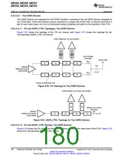
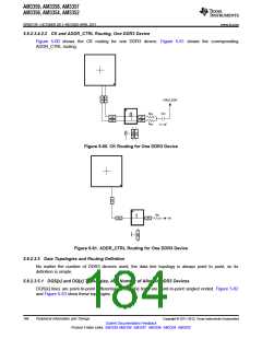
5.6.2.3.4.1 Two DDR3 Devices
Two DDR3 devices are supported on the DDR3 interface consisting of two x8 DDR3 devices arranged as
one 16-bit bank. These two devices may be mounted on a single side of the PCB, or may be mirrored in a
pair to save board space at a cost of increased routing complexity and parts on the backside of the PCB.
5.6.2.3.4.1.1 CK and ADDR_CTRL Topologies, Two DDR3 Devices
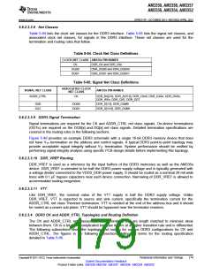
Figure 5-52 shows the topology of the CK net classes and Figure 5-53 shows the topology for the
corresponding ADDR_CTRL net classes.
DDR3 Differential CK Input Buffers
–
–
+
+
Clock Parallel
Terminator
VDDS_DDR
Rcp
A1
A1
A2
A2
A3
A3
AT
AT
Cac
AM335x
Differential Clock
Output Buffer
+
–
0.1 µF
Rcp
Routed as Differential Pair
Figure 5-52. CK Topology for Two DDR3 Devices
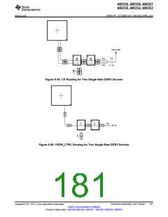
DDR3 Address and Control Input Buffers
Address and Control
Terminator
Rtt
AM335x
Address and Control
Output Buffer
A1
A2
A3
AT
Vtt
Figure 5-53. ADDR_CTRL Topology for Two DDR3 Devices
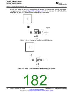
5.6.2.3.4.1.2 CK and ADDR_CTRL Routing, Two DDR3 Devices
Figure 5-54 shows the CK routing for two DDR3 devices placed on the same side of the PCB. Figure 5-55
shows the corresponding ADDR_CTRL routing.
180
Peripheral Information and Timings
Copyright © 2011–2013, Texas Instruments Incorporated
Submit Documentation Feedback
Product Folder Links: AM3359 AM3358 AM3357 AM3356 AM3354 AM3352

 TI [ TEXAS INSTRUMENTS ]