AM3359, AM3358, AM3357
AM3356, AM3354, AM3352
www.ti.com
SPRS717F –OCTOBER 2011–REVISED APRIL 2013
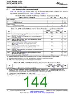
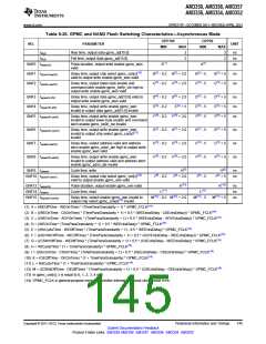
Table 5-30. GPMC and NAND Flash Switching Characteristics—Asynchronous Mode
OPP100
MIN
OPP50
MIN
NO.
PARAMETER
UNIT
MAX
MAX
tR(d)
Rise time, output data gpmc_ad[15:0]
Fall time, output data gpmc_ad[15:0]
2
2
2
2
ns
ns
ns
tF(d)
GNF0 tw(wenV)
Pulse duration, output write enable gpmc_wen
valid
Delay time, output chip select gpmc_csn[x](13)
valid to output write enable gpmc_wen valid
A(1)
A(1)
B(2) - 5
C(3) - 5
GNF1 td(csnV-wenV)
GNF2 tw(cleH-wenV)
B(2) - 0.2
B(2) + 2.0
B(2) + 5
C(3) + 5
ns
ns
Delay time, output lower-byte enable and
command latch enable gpmc_be0n_cle high to
output write enable gpmc_wen valid
C(3) - 0.2 C(3) + 2.0
D(4) - 0.2 D(4) + 2.0
GNF3 tw(wenV-dV)
GNF4 tw(wenIV-dIV)
GNF5 tw(wenIV-cleIV)
Delay time, output data gpmc_ad[15:0] valid to
output write enable gpmc_wen valid
D(4) - 5
E(5) - 5
F(6) - 5
D(4) + 5
E(5) + 5
F(6) + 5
ns
ns
ns
Delay time, output write enable gpmc_wen
invalid to output data gpmc_ad[15:0] invalid
E(5) - 0.2
F(6) - 0.2
E(5) + 5
Delay time, output write enable gpmc_wen
invalid to output lower-byte enable and command
latch enable gpmc_be0n_cle invalid
F(6) + 2.0
GNF6 tw(wenIV-csnIV)
GNF7 tw(aleH-wenV)
GNF8 tw(wenIV-aleIV)
Delay time, output write enable gpmc_wen
invalid to output chip select gpmc_csn[x](13)
invalid
G(7) - 0.2 G(7) + 2.0
C(3) - 0.2 C(3) + 2.0
G(7) - 5
C(3) - 5
F(6) - 5
G(7) + 5
C(3) + 5
F(6) + 5
ns
ns
ns
Delay time, output address valid and address
latch enable gpmc_advn_ale high to output write
enable gpmc_wen valid
Delay time, output write enable gpmc_wen
invalid to output address valid and address latch
enable gpmc_advn_ale invalid
F(6) - 0.2
F(6) + 2.0
GNF9 tc(wen)
Cycle time, write
Delay time, output chip select gpmc_csn[x](13)
valid to output enable gpmc_oen valid
H(8)
I(9) + 2.0
H(8)
I(9) + 5
ns
ns
GNF10 td(csnV-oenV)
I(9) - 0.2
I(9) - 5
GNF13 tw(oenV)
GNF14 tc(oen)
Pulse duration, output enable gpmc_oen valid
Cycle time, read
K(10)
K(10)
ns
ns
ns
L(11)
M(12) - 0.2 M(12) + 2.0
L(11)
M(12) - 5
GNF15 tw(oenIV-csnIV)
Delay time, output enable gpmc_oen invalid to
output chip select gpmc_csn[x](13) invalid
M(12) + 5
(1) A = (WEOffTime - WEOnTime) * (TimeParaGranularity + 1) * GPMC_FCLK(14)
(2) B = ((WEOnTime - CSOnTime) * (TimeParaGranularity + 1) + 0.5 * (WEExtraDelay - CSExtraDelay)) * GPMC_FCLK(14)
(3) C = ((WEOnTime - ADVOnTime) * (TimeParaGranularity + 1) + 0.5 * (WEExtraDelay - ADVExtraDelay)) * GPMC_FCLK(14)
(4) D = (WEOnTime * (TimeParaGranularity + 1) + 0.5 * WEExtraDelay) * GPMC_FCLK(14)
(5) E = ((WrCycleTime - WEOffTime) * (TimeParaGranularity + 1) - 0.5 * WEExtraDelay) * GPMC_FCLK(14)
(6) F = ((ADVWrOffTime - WEOffTime) * (TimeParaGranularity + 1) + 0.5 * (ADVExtraDelay - WEExtraDelay)) * GPMC_FCLK(14)
(7) G = ((CSWrOffTime - WEOffTime) * (TimeParaGranularity + 1) + 0.5 * (CSExtraDelay - WEExtraDelay)) * GPMC_FCLK(14)
(8) H = WrCycleTime * (1 + TimeParaGranularity) * GPMC_FCLK(14)
(9) I = ((OEOnTime - CSOnTime) * (TimeParaGranularity + 1) + 0.5 * (OEExtraDelay - CSExtraDelay)) * GPMC_FCLK(14)
(10) K = (OEOffTime - OEOnTime) * (1 + TimeParaGranularity) * GPMC_FCLK(14)
(11) L = RdCycleTime * (1 + TimeParaGranularity) * GPMC_FCLK(14)
(12) M = ((CSRdOffTime - OEOffTime) * (TimeParaGranularity + 1) + 0.5 * (CSExtraDelay - OEExtraDelay)) * GPMC_FCLK(14)
(13) In gpmc_csn[x], x is equal to 0, 1, 2, 3, 4 or 5.
(14) GPMC_FCLK is general-purpose memory controller internal functional clock period in ns.
Copyright © 2011–2013, Texas Instruments Incorporated
Peripheral Information and Timings
145
Submit Documentation Feedback
Product Folder Links: AM3359 AM3358 AM3357 AM3356 AM3354 AM3352

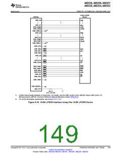
 TI [ TEXAS INSTRUMENTS ]