AM3359, AM3358, AM3357
AM3356, AM3354, AM3352
SPRS717F –OCTOBER 2011–REVISED APRIL 2013
www.ti.com
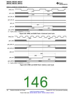
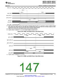
5.6.1.3 GPMC and NAND Flash—Asynchronous Mode
Table 5-28 and Table 5-29 assume testing over the recommended operating conditions and electrical
characteristic conditions below (see Figure 5-28 through Figure 5-31).
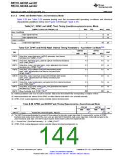
Table 5-27. GPMC and NAND Flash Timing Conditions—Asynchronous Mode
TIMING CONDITION PARAMETER
MIN
TYP
MAX
UNIT
Input Conditions
tR
tF
Input signal rise time
Input signal fall time
1
1
5
5
ns
ns
Output Condition
CLOAD
Output load capacitance
3
30
pF
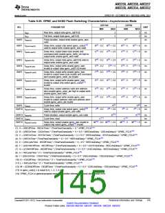
Table 5-28. GPMC and NAND Flash Internal Timing Parameters—Asynchronous Mode(1)(2)
OPP100
MIN
OPP50
MIN
NO.
UNIT
MAX
MAX
GNFI1 Delay time, output data gpmc_ad[15:0] generation from internal
functional clock GPMC_FCLK(3)
6.5
6.5
ns
GNFI2 Delay time, input data gpmc_ad[15:0] capture from internal functional
clock GPMC_FCLK(3)
4.0
6.5
6.5
4.0
6.5
6.5
ns
ns
ns
GNFI3 Delay time, output chip select gpmc_csn[x] generation from internal
functional clock GPMC_FCLK(3)
GNFI4 Delay time, output address valid and address latch enable
gpmc_advn_ale generation from internal functional clock
GPMC_FCLK(3)
GNFI5 Delay time, output lower-byte enable and command latch enable
gpmc_be0n_cle generation from internal functional clock
GPMC_FCLK(3)
6.5
6.5
ns
GNFI6 Delay time, output enable gpmc_oen generation from internal functional
clock GPMC_FCLK(3)
6.5
6.5
6.5
6.5
ns
ns
ps
GNFI7 Delay time, output write enable gpmc_wen generation from internal
functional clock GPMC_FCLK(3)
GNFI8 Skew, functional clock GPMC_FCLK(3)
100
100
(1) Internal parameters table must be used to calculate data access time stored in the corresponding CS register bit field.
(2) Internal parameters are referred to the GPMC functional internal clock which is not provided externally.
(3) GPMC_FCLK is general-purpose memory controller internal functional clock.
Table 5-29. GPMC and NAND Flash Timing Requirements—Asynchronous Mode
OPP100
MIN
OPP50
MIN
NO.
UNIT
MAX
J(2)
MAX
J(2)
GNF12(1) tacc(d)
Access time, input data gpmc_ad[15:0]
ns
(1) The GNF12 parameter illustrates the amount of time required to internally sample input data. It is expressed in number of GPMC
functional clock cycles. From start of the read cycle and after GNF12 functional clock cycles, input data is internally sampled by the
active functional clock edge. The GNF12 value must be stored inside AccessTime register bit field.
(2) J = AccessTime * (TimeParaGranularity + 1) * GPMC_FCLK(3)
(3) GPMC_FCLK is general-purpose memory controller internal functional clock period in ns.
144
Peripheral Information and Timings
Copyright © 2011–2013, Texas Instruments Incorporated
Submit Documentation Feedback
Product Folder Links: AM3359 AM3358 AM3357 AM3356 AM3354 AM3352

 TI [ TEXAS INSTRUMENTS ]