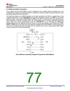
ADS131M04-Q1
ZHCSOL7A –MARCH 2022 –REVISED AUGUST 2022
www.ti.com.cn
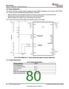
9.2.2 Detailed Design Procedure
The following sections provide guidelines for selecting the external components and the configuration of the
ADS131M04-Q1 for the various measurements in this application example.
9.2.2.1 Current Shunt Measurement
In a typical BMS, the current through the shunt resistor must be measured in both directions for charging and
discharging the battery pack. In an overcurrent or short-circuit condition, the current can be as high as IBAT_MAX
=
±5 kA in this example application. Therefore, the maximum voltage drop across the shunt is up to VSHUNT
=
RSHUNT × IBAT_MAX = 35 μΩ × ±4 kA = ±140 mV.
To measure this shunt voltage, configure channel 1 of the ADS131M04-Q1 for gain = 8, which allows differential
voltage measurements of VIN1 = VAIN1P – VAIN1N = ±VREF / 8 = ±1.2 V / 8 = ±150 mV. The integrated charge
pump in the device allows voltage measurements 1.3 V below AGND while using a unipolar analog power
supply. This bipolar voltage measurement capability is important because one side of the shunt is connected to
the same GND potential as the AGND pin of the ADS131M04-Q1, which means that the absolute voltage that
the device must measure is up to 140 mV below AGND.
To enable fast overcurrent detection within 1 ms while providing high accuracy and resolution, operate the
ADS131M04-Q1 at 4 kSPS (OSR = 1024, high-resolution mode) using global-chop mode. Global-chop mode
enables measurements with minimal offset error over temperature and time. The conversion time using these
settings is 0.754 ms according to 方程式 9. The input-referred noise is approximately 2.70 μVRMS / √2 =
1.91 μVRMS following the explanations in the Noise Measurements section. Thus, currents as small as 1.91
μVRMS / 35 μΩ = 55 mA can be resolved. The resolution can be further improved by averaging the conversion
results over a longer period of time in the microcontroller that interfaces with the ADS131M04-Q1.
9.2.2.2 Battery Pack Voltage Measurement
The 800-V battery-pack voltage is divided down to the voltage range of the ADS131M04-Q1 using a high-voltage
resistor divider (RH1, RH2, RH3, and RL). Gain = 1 is used for channel 0 in this case to allow differential voltage
measurements of VIN0 = VAIN0P – VAIN0N = ±1.2 V. The battery-pack voltage measurement is a unipolar, single-
ended measurement. Thus, only the voltage range from 0 V to 1.2 V of the ADS131M04-Q1 is used. 方程式 11
calculates the resistor divider ratio.
VIN / VBAT_MAX = 1.2 V / 800 V = RL / (RL + RH1 + RH2 + RH3
)
(11)
The leakage current drawn by the resistor divider must be less than 100 μA in this example to avoid
unnecessarily draining the battery. The resistance of the divider must therefore be larger than RTOTAL
≥
VBAT_MAX / ILEAKAGE = 800 V / 100 μA = 8 MΩ. The resistor values are chosen as RH1 = RH2 = RH3 = 2.8 MΩ
and RL = 12.4 kΩ. Thus, the maximum voltage across RL is 1.18 V at VBAT_MAX = 800 V, leaving some
headroom to the maximum input voltage of 1.2 V of the ADS131M04-Q1.
The maximum resistance of a single resistor that can be used in an automotive circuit design is often limited to a
certain value. Also, the maximum voltage a single resistor can withstand is limited. These reasons are why the
high-side resistor of the divider is split into multiple resistors (RH1, RH2, and RH3). Another reason is that in case
a single resistor has a short-circuit fault, the remaining resistors still limit the current into the ADS131M04-Q1
analog input pin (AIN0P) to safe levels.
Copyright © 2022 Texas Instruments Incorporated
Submit Document Feedback
81
Product Folder Links: ADS131M04-Q1

 TI [ TEXAS INSTRUMENTS ]