ADS131M04-Q1
ZHCSOL7A –MARCH 2022 –REVISED AUGUST 2022
www.ti.com.cn
9.3 Power Supply Recommendations
9.3.1 CAP Pin Behavior
The ADS131M04-Q1 core digital voltage of 1.8 V is created from an internal LDO from DVDD. The CAP pin
outputs the LDO voltage created from the DVDD supply and requires an external bypass capacitor. When
operating from DVDD > 2.7 V, place a 220-nF capacitor on the CAP pin to DGND. If DVDD ≤ 2 V, tie the CAP
pin directly to the DVDD pin and decouple the star-connected pins using a 100-nF capacitor to DGND.
9.3.2 Power-Supply Sequencing
The power supplies can be sequenced in any order but the analog and digital inputs must never exceed the
respective analog or digital power-supply voltage limits.
9.3.3 Power-Supply Decoupling
Good power-supply decoupling is important to achieve optimum performance. AVDD and DVDD must each be
decoupled with a 1-µF capacitor. Place the bypass capacitors as close to the power-supply pins of the device as
possible with low-impedance connections. Using multilayer ceramic chip capacitors (MLCCs) that offer low
equivalent series resistance (ESR) and inductance (ESL) characteristics are recommended for power-supply
decoupling purposes. For very sensitive systems, or for systems in harsh noise environments, avoiding the use
of vias for connecting the capacitors to the device pins can offer superior noise immunity. The use of multiple
vias in parallel lowers the overall inductance and is beneficial for connections to ground planes. The analog and
digital ground are recommended to be connected together as close to the device as possible.
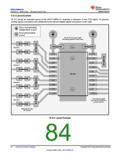
9.4 Layout
9.4.1 Layout Guidelines
For best performance, dedicate an entire PCB layer to a ground plane and do not route any other signal traces
on this layer. However, depending on restrictions imposed by specific end equipment, a dedicated ground plane
may not be practical. If ground plane separation is necessary, make a direct connection of the planes at the
ADC. Do not connect individual ground planes at multiple locations because this configuration creates ground
loops.
Route digital traces away from all analog inputs and associated components in order to minimize interference.
Use C0G capacitors on the analog inputs. Use ceramic capacitors (for example, X7R grade) for the power-
supply decoupling capacitors. High-K capacitors (Y5V) are not recommended. Place the required capacitors as
close as possible to the device pins using short, direct traces. For optimum performance, use low-impedance
connections on the ground-side connections of the bypass capacitors.
When applying an external clock, be sure the clock is free of overshoot and glitches. A source-termination
resistor placed at the clock buffer often helps reduce overshoot. Glitches present on the clock input can lead to
noise within the conversion data.
Copyright © 2022 Texas Instruments Incorporated
Submit Document Feedback
83
Product Folder Links: ADS131M04-Q1

 TI [ TEXAS INSTRUMENTS ]