ADS131B04-Q1
ZHCSMK3B –NOVEMBER 2020 –REVISED NOVEMBER 2021
www.ti.com.cn
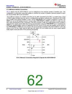
9.1.4 Minimum Interface Connections
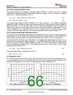
图 9-2 depicts how the ADS131B04-Q1 can be configured for the minimum number of interface pins. This
configuration is useful when using data isolation to minimize the number of isolation channels required or when
the microcontroller (MCU) pins are limited.
The CLKIN pin requires an LVCMOS clock that can be either generated by the MCU or created using a local
LVCMOS output oscillator when the device is configured for use with an external clock. Otherwise tie the CLKIN
pin to DGND if the internal oscillator is used. Tie the SYNC/RESET pin to DVDD in hardware if unused. The
DRDY pin can be left floating if unused. Connect either SYNC/RESET or DRDY to the MCU to make sure the
MCU stays synchronized to ADC conversions. If the MCU provides CLKIN, the CLKIN periods can be counted to
determine the sample period rather than forcing synchronization using the SYNC/RESET pin or monitoring the
DRDY pin. Synchronization cannot be regained if a bit error occurs on the clock and samples can be missed if
the SYNC/RESET or DRDY pins are not used. CS can be tied low in hardware if the ADS131B04-Q1 is the only
device on the SPI bus. Make sure the data input and output CRC are enabled and are used to guard against
faulty register reads and writes if CS is tied low permanently.
Local
Oscillator
DVDD
OR
CLKIN
SYNC/RESET
DRDY
CLKOUT
GPIO
GPIO
CS
OR
Device
MCU
CS
SCLK
DIN
OR
SCLK
MOSI
MISO
DOUT
DGND
图9-2. Minimum Connections Required to Operate the ADS131B04-Q1
Copyright © 2022 Texas Instruments Incorporated
62
Submit Document Feedback
Product Folder Links: ADS131B04-Q1

 TI [ TEXAS INSTRUMENTS ]