ADS131B04-Q1
ZHCSMK3B –NOVEMBER 2020 –REVISED NOVEMBER 2021
www.ti.com.cn
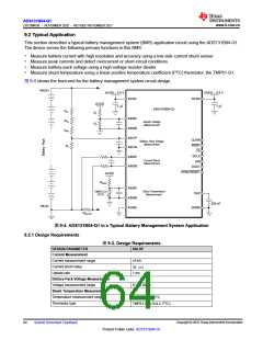
9.2.2.3 Shunt Temperature Measurement
The shunt temperature in this example is measured using the TMP61-Q1, a linear 10-kΩ PTC, in a typical
voltage divider configuration using the analog supply (AVDD) as excitation. The PTC resistance is calculated
using 方程式11, which is derived from 方程式10:
VIN3 = VAIN3P –VAIN3N = AVDD x RPTC / (RBIAS + RPTC
)
(10)
(11)
RPTC = RBIAS x VIN3 / (AVDD –VIN3
)
The maximum input voltage on AIN3P is limited to 1.2 V when using gain = 1 for channel 3 with AIN3N
connected to AGND. Therefore the value of the precision resistor, RBIAS, must be chosen so that the voltage on
AIN3P stays below 1.2 V for the value range of the PTC across the temperature range that needs to be
measured. The TMP61-Q1 has its largest resistance at the most positive temperature, approximately 18 kΩ at
+125°C. Following 方程式 11, that means RBIAS ≥ 31.5 kΩ. A value of 36.5 kΩ is chosen for RBIAS to allow
variation in the AVDD supply voltage up to 3.6 V without exceeding the maximum AIN3P voltage of 1.2 V.
9.2.2.4 Auxiliary Analog Supply Voltage Measurement
The accuracy of the analog supply directly impacts the measurement accuracy of the PTC in this measurement
implementation. In order to increase the temperature measurement accuracy, channel 0 of ADS131B04-Q1 is
used to measure the analog supply. The measured AVDD value is then used in 方程式11 to calculate RPTC
.
A resistor divider (R1 and R2) is used to attenuate the 3.3-V analog supply voltage down to less than 1.2 V so
that channel 0 can measure the voltage using gain = 1 with AIN0N connected to AGND. The resistor divider
needs to be chosen so that the voltage on AIN0P stays below 1.2 V at the maximum AVDD voltage that can
occur in the application. Following 方程式 12, the resistors are chosen as R1 = 20 kΩ and R2 = 10 kΩ to allow
measurements up to AVDD = 3.6 V.
VIN0 = VAIN0P –VAIN0N = AVDD x R2 / (R1 + R2)
(12)
The analog supply voltage is calculated using 方程式13:
AVDD = VIN0 x (1 + R1 / R2)
(13)
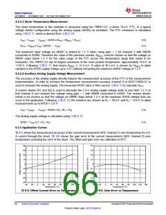
9.2.3 Application Curves
图9-5 shows the measurement accuracy of the current measurement (ADC channel 2) over temperature for a 0-
A current through the shunt. 图 9-6 shows the gain error of the current measurement (ADC channel 2) over
temperature excluding the error of the shunt. The offset and gain error are calibrated at 25°C.
40
30
0.4
0.3
0.2
0.1
0
20
10
0
-10
-20
-30
-40
-0.1
-0.2
-0.3
-0.4
-40
-20
0
20
40 60
Temperature (°C)
80
100 120 140
-40
-20
0
20
40 60
Temperature (°C)
80
100 120 140
图9-5. Offset Current Error vs Temperature
图9-6. Gain Error vs Temperature
Copyright © 2022 Texas Instruments Incorporated
66
Submit Document Feedback
Product Folder Links: ADS131B04-Q1

 TI [ TEXAS INSTRUMENTS ]