ADS131B04-Q1
ZHCSMK3B –NOVEMBER 2020 –REVISED NOVEMBER 2021
www.ti.com.cn
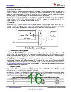
To switch between a running CLKIN and the internal oscillator as the MCLK source, put the device in standby
mode to avoid creating glitches when switching the clock source because there are no clock sequencers in the
device. Likewise, put the device in standby mode before changing power modes because a change in power
mode changes the MCLK frequency based on the clock divider setting.
When always using the internal oscillator as the MCLK source, tie the CLKIN pin to DGND. Tying the CLKIN pin
to DGND avoids the need to enter standby mode when switching from an external clock to the internal oscillator
at power-up or after a reset.
8.3.7 ΔΣModulator
The ADS131B04-Q1 uses a delta-sigma (ΔΣ) modulator to convert the analog input voltage to a one's density
modulated digital bit-stream. The ΔΣ modulator oversamples the input voltage at a frequency many times
greater than the output data rate. The modulator frequency, fMOD, of the ADS131B04-Q1 is equal to half the
main clock frequency (that is, fMOD = fMCLK / 2).
The output of the modulator is fed back to the modulator input through a digital-to-analog converter (DAC) as a
means of error correction. This feedback mechanism shapes the modulator quantization noise in the frequency
domain to make the noise more dense at higher frequencies and less dense in the band of interest. The digital
decimation filter following the ΔΣ modulator significantly attenuates the out-of-band modulator quantization
noise, allowing the device to provide excellent dynamic range.
8.3.8 Digital Filter
The ΔΣmodulator bit-stream feeds into a digital filter. The digital filter is a linear phase, finite impulse response
(FIR), low-pass sinc-type filter that attenuates the out-of-band quantization noise of the ΔΣ modulator. The
digital filter demodulates the output of the ΔΣ modulator by averaging. The data passing through the filter is
decimated and downsampled, to reduce the rate at which data come out of the modulator (fMOD) to the output
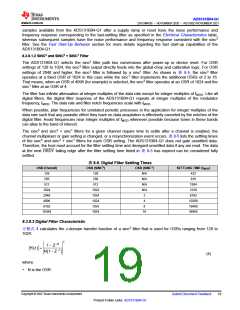
data rate (fDATA). The decimation factor, defined as per 方程式3, is called the oversampling ratio (OSR).
OSR = fMOD / fDATA
(3)
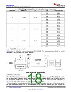
The OSR is configurable and is set by the OSR[2:0] bits in the CLOCK register. There are eight OSR settings in
the ADS131B04-Q1, allowing eight different data rate settings for any given main clock frequency. 表8-4 lists the
OSR settings and their corresponding output data rates for the nominal MCLK frequencies mentioned.
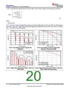
The OSR determines the amount of averaging of the modulator output in the digital filter and therefore also the
filter bandwidth. The filter bandwidth directly affects the noise performance of the ADC because lower bandwidth
results in lower noise, whereas higher bandwidth results in higher noise. See 表 7-1 for the noise specifications
for various OSR settings.
Copyright © 2022 Texas Instruments Incorporated
Submit Document Feedback
17
Product Folder Links: ADS131B04-Q1

 TI [ TEXAS INSTRUMENTS ]