ADS131B04-Q1
ZHCSMK3B –NOVEMBER 2020 –REVISED NOVEMBER 2021
www.ti.com.cn
8 Detailed Description
8.1 Overview
The ADS131B04-Q1 is a low-power, four-channel, simultaneous-sampling, 24-bit, delta-sigma (ΔΣ) analog-to-
digital converter (ADC) with a low-drift internal reference voltage. The dynamic range, size, feature set, and
power consumption are optimized for cost-sensitive applications requiring simultaneous sampling.
The ADS131B04-Q1 requires both analog and digital supplies. The analog power supply (AVDD – AGND) can
operate between 2.7 V and 3.6 V. An integrated negative charge pump allows absolute input voltages as low as
0.3 V below AGND, which enables measurements of input signals varying around ground with a unipolar power
supply. The digital power supply (DVDD – DGND) can operate between 2.7 V and 3.6 V. The device features a
high input impedance programmable gain amplifier (PGA) with gains up to 128. The ADC receives its reference
voltage from an integrated 1.2-V reference. The device allows differential input voltages as large as the
reference. Three power-scaling modes allow designers to trade power consumption for noise performance.
Each channel on the ADS131B04-Q1 contains a digital decimation filter that demodulates the output of the ΔΣ
modulators. The filter enables data rates as high as 32 kSPS per channel in high-resolution mode. Offset and
gain calibration registers can be programmed to automatically adjust output samples for measured offset and
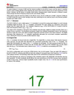
gain errors. The Functional Block Diagram provides a detailed diagram of the ADS131B04-Q1.
The device communicates via a serial peripheral interface (SPI)-compatible interface. Several SPI commands
and internal registers control the operation of the ADS131B04-Q1. Other devices can be added to the same SPI
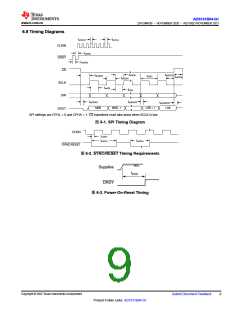
bus by adding discrete CS control lines. The SYNC/RESET pin can be used to synchronize conversions
between multiple ADS131B04-Q1 devices as well as to maintain synchronization with external events.
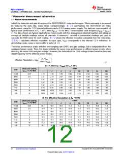
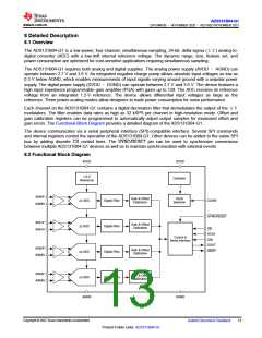
8.2 Functional Block Diagram
AVDD
DVDD
1.2-V
Reference
Oscillator
AIN0P
AIN0N
+
Gain & Offset
Calibration
Clock
Selection
DS ADC
DS ADC
DS ADC
Digital Filter
Digital Filter
Digital Filter
Digital Filter
CLKIN
œ
SYNC/RESET
AIN1P
AIN1N
+
Gain & Offset
Calibration
CS
œ
SCLK
Control &
Serial Interface
DIN
DOUT
DRDY
AIN2P
AIN2N
+
Gain & Offset
Calibration
œ
AIN3P
AIN3N
+
Gain & Offset
Calibration
DS ADC
œ
AGND
DGND
Copyright © 2022 Texas Instruments Incorporated
Submit Document Feedback
13
Product Folder Links: ADS131B04-Q1

 TI [ TEXAS INSTRUMENTS ]