ADS131B04-Q1
ZHCSMK3B –NOVEMBER 2020 –REVISED NOVEMBER 2021
www.ti.com.cn
8.3.5 Internal Test Signals
The ADS131B04-Q1 features an internal analog test signal that is useful for troubleshooting and diagnosis. A
positive or negative dc test signal can be applied to the channel inputs through the input multiplexer. The
multiplexer is controlled through the MUXn[1:0] bits in the CHn_CFG register. The test signals are created by
internally dividing the reference voltage. The same signal is shared by all channels.
The test signal is nominally 2 / 15 × VREF. The test signal automatically adjusts its voltage level with the gain
setting such that the ADC always measures a signal that is 2 / 15 × VDiff Max. For example, at a gain of 1, this
voltage equates to 160 mV. At a gain of 2, this voltage is 80 mV.
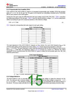
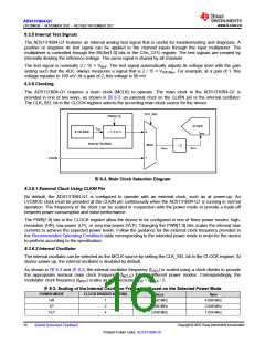
8.3.6 Clocking
The ADS131B04-Q1 requires a main clock (MCLK) to operate. The main clock to the ADS131B04-Q1 is
provided in one of two ways, as shown in 图 8-3: an external clock on the CLKIN pin or the internal oscillator.
The CLK_SEL bit in the CLOCK register selects the according main clock source for the device.
CLK_SEL
PWR[1:0]
DS ADC
fOSC
8.192 MHz
÷ 1, 2 or 4
0
fMOD
Internal Oscillator
MUX
÷ 2
fMOD
fMCLK
1
CLKIN
图8-3. Main Clock Selection Diagram
8.3.6.1 External Clock Using CLKIN Pin
By default, the ADS131B04-Q1 is configured to operate with an external clock, such as at power-up. An
LVCMOS clock must be provided at the CLKIN pin continuously when the ADS131B04-Q1 is running in normal
operation. The frequency of the clock can be scaled in conjunction with the power mode to provide a trade-off
between power consumption and noise performance.
The PWR[1:0] bits in the CLOCK register allow the device to be configured in one of three power modes: high-
resolution (HR), low-power (LP), or very-low-power (VLP). Changing the PWR[1:0] bits scales the internal bias
currents to achieve the expected power levels. Follow the guidance for the external clock frequency provided in
the Recommended Operating Conditions table corresponding to the intended power mode in order for the device
to perform according to the specification.
8.3.6.2 Internal Oscillator
The internal oscillator can be selected as the MCLK source by setting the CLK_SEL bit in the CLOCK register. At
device power-up, the internal oscillator is disabled by default.
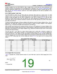
As shown in 图 8-3 and 表 8-3, the internal oscillator frequency (fOSC) is scaled using a clock divider to provide
the appropriate nominal main clock frequency (fMCLK) for the different power modes. Correspondingly, the
modulator clock frequency (fMOD) scales as well because fMOD = fMCLK / 2.
表8-3. Scaling of the Internal Oscillator Frequency Based on the Selected Power Mode
POWER MODE
CLOCK DIVIDER SETTING
fMCLK
fMOD
HR
LP
1
2
4
8.192 MHz
4.096 MHz
2.048 MHz
4.096 MHz
2.048 MHz
1.024 MHz
VLP
Copyright © 2022 Texas Instruments Incorporated
16
Submit Document Feedback
Product Folder Links: ADS131B04-Q1

 TI [ TEXAS INSTRUMENTS ]