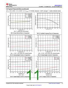
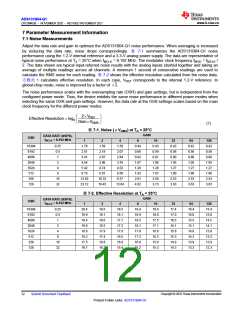
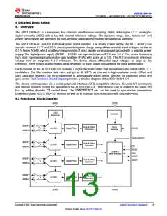
ADS131B04-Q1
ZHCSMK3B –NOVEMBER 2020 –REVISED NOVEMBER 2021
www.ti.com.cn
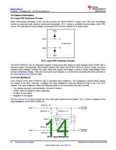
8.3.3 Programmable Gain Amplifier (PGA)
Each channel of the ADS131B04-Q1 features an integrated programmable gain amplifier (PGA) that provides
gains of 1, 2, 4, 8, 16, 32, 64, and 128. The gains for all channels are individually controlled by the PGAGAINn
bits for each channel in the GAIN register.
Varying the PGA gain scales the differential full-scale input voltage range (FSR) of the ADC. 方程式 2 describes
the relationship between FSR and gain. 方程式 2 uses the internal reference voltage, 1.2 V, as the scaling factor
without accounting for gain error caused by tolerance in the reference voltage.
FSR = ±1.2 V / Gain
(2)
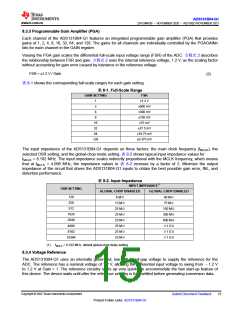
表8-1 shows the corresponding full-scale ranges for each gain setting.
表8-1. Full-Scale Range
GAIN SETTING
FSR
1
2
±1.2 V
±600 mV
±300 mV
±150 mV
±75 mV
4
8
16
32
64
128
±37.5 mV
±18.75 mV
±9.375 mV
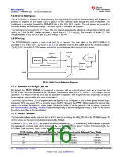
The input impedance of the ADS131B04-Q1 depends on three factors: the main clock frequency (fMCLK), the
selected OSR setting, and the global-chop mode setting. 表8-2 shows typical input impedance values for
fMCLK = 8.192 MHz. The input impedance scales indirectly proportional with the MCLK frequency, which means
that at fMCLK = 4.096 MHz, the impedance values in 表 8-2 increase by a factor of 2. Minimize the output
impedance of the circuit that drives the ADS131B04-Q1 inputs to obtain the best possible gain error, INL, and
distortion performance.
表8-2. Input Impedance
INPUT IMPEDANCE(1)
OSR SETTING
GLOBAL-CHOP DISABLED
GLOBAL-CHOP ENABLED
128
256
6 MΩ
13 MΩ
25 MΩ
25 MΩ
25 MΩ
25 MΩ
25 MΩ
25 MΩ
40 MΩ
75 MΩ
512
150 MΩ
1024
2048
4096
8192
16384
300 MΩ
600 MΩ
≥1 GΩ
≥1 GΩ
≥1 GΩ
(1) fMCLK = 8.192 MHz, default global-chop delay setting.
8.3.4 Voltage Reference
The ADS131B04-Q1 uses an internally generated, low-drift, band-gap voltage to supply the reference for the
ADC. The reference has a nominal voltage of 1.2 V, allowing the differential input voltage to swing from –1.2 V
to 1.2 V at Gain = 1. The reference circuitry starts up very quickly to accommodate the fast start-up feature of
this device. The device waits until after the reference circuitry is fully settled before generating conversion data.
Copyright © 2022 Texas Instruments Incorporated
Submit Document Feedback
15
Product Folder Links: ADS131B04-Q1

 TI [ TEXAS INSTRUMENTS ]