ADS1291
ADS1292
ADS1292R
SBAS502A –DECEMBER 2011–REVISED MARCH 2012
www.ti.com
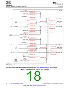
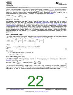
Special care must be taken in PCB layout to minimize the parasitic capacitance CP1/CP2. The absolute value of
these capacitances must be less than 20 pF. Ideally, CFILTER should be placed right at the pins to minimize these
capacitors. Mismatch between these capacitors will lead to CMRR degradation. Assuming everything else is
perfectly matched, the 60-Hz CMRR as a function of this mismatch is given by Equation 5.
Gain
CMRR = 20log
2p ´ 2e3 ´ DC ´ 60
P
(5)
where ΔCP = CP1 – CP2
For example, a mismatch of 20 pF with a gain of 6 limits the CMRR to 112 dB. If ΔCP is small, then the CMRR is
limited by the PGA itself and is as specified in the Electrical Characteristics table. The PGA are chopped
internally at either 8, 32, or 64 kSPS, as determined by the CHOP bits (see the RLD_SENS: Right Leg Drive
Sense Selection register, bits[7:6]). The digital decimation filter filters out the chopping ripple in the normal path
so the chopping ripple is not a concern. If PGA output is used for hardware PACE detection, the chopping ripple
must be filtered. First-order filtering is provided by the RC filter at the PGA output. Additional filtering may be
needed to suppress the chopping ripple. If the PGA output is routed to other circuitry, a 20-kΩ series resistance
must be added in the path near the CFILTER capacitor. The routing should be matched to maintain the CMRR
performance.
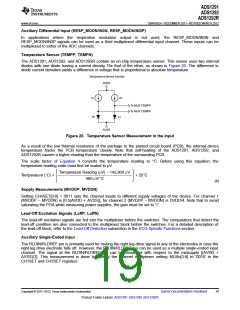
Input Common-Mode Range
The usable input common-mode range of the front end depends on various parameters, including the maximum
differential input signal, supply voltage, and PGA gain. Equation 6 describes this range.
Gain VMAX_DIFF
Gain VMAX_DIFF
AVDD - 0.2 -
> CM > AVSS + 0.2 +
2
2
where:
VMAX_DIFF = maximum differential signal at the input of the PGA
CM = common-mode range
(6)
For example:
If VDD = 3 V, gain = 6, and VMAX_DIFF = 350 mV
Then 1.25 V < CM < 1.75 V
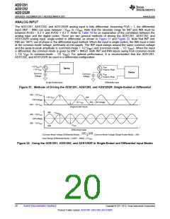
Input Differential Dynamic Range
The differential (INP – INN) signal range depends on the analog supply and reference used in the system.
Equation 7 shows this range.
VREF
±VREF 2 VREF
=
Max (INP - INN) <
;
Full-Scale Range =
Gain
Gain
Gain
(7)
The 3-V supply, with a reference of 2.42 V and a gain of 6 for ECGs, is optimized for power with a differential
input signal of approximately 300 mV. For higher dynamic range, a 5-V supply with a reference of 4.033 V (set
by the VREF_4V bit of the CONFIG2 register) can be used to increase the differential dynamic range.
22
Submit Documentation Feedback
Copyright © 2011–2012, Texas Instruments Incorporated
Product Folder Link(s): ADS1291 ADS1292 ADS1292R

 TI [ TEXAS INSTRUMENTS ]