ADS1115-Q1
SBAS563 –DECEMBER 2011
www.ti.com
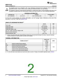
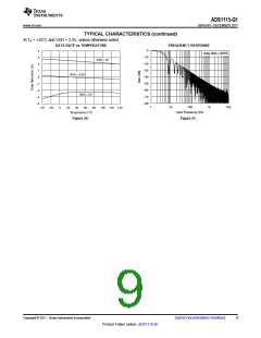
ELECTRICAL CHARACTERISTICS (continued)
All specifications at –40°C to +125°C, VDD = 3.3V, and Full-Scale (FS) = ±2.048V, unless otherwise noted.
Typical values are at +25°C, TA = TJ
ADS1115-Q1
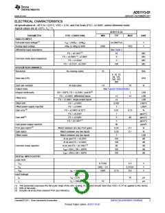
PARAMETER
POWER-SUPPLY REQUIREMENTS
Power-supply voltage
TEST CONDITIONS
MIN
TYP
MAX
UNIT
2
5.5
2
V
Power-down current at 25°C
Power-down current up to 125°C
Operating current at 25°C
Operating current up to 125°C
VDD = 5.0V
0.5
μA
5
μA
Supply current
150
200
300
μA
μA
0.9
0.5
0.3
mW
mW
mW
Power dissipation
VDD = 3.3V
VDD = 2.0V
TEMPERATURE
Storage temperature
–60
–40
+150
+125
°C
°C
Specified ambient temperature
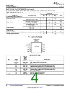
PIN CONFIGURATIONS
DGS PACKAGE
MSOP-10
(TOP VIEW)
ADDR
ALERT/RDY
GND
1
2
3
4
5
10 SCL
9
8
7
6
SDA
VDD
AIN3
AIN2
ADS1115-Q1
AIN0
AIN1
PIN DESCRIPTIONS
ANALOG/
DIGITAL
INPUT/
PIN #
DEVICE
ADDR
ALERT/RDY
GND
OUTPUT
DESCRIPTION
I2C slave address select
1
2
Digital Input
Digital Output
Analog
Digital comparator output or conversion ready
Ground
3
4
AIN0
Analog Input
Analog Input
Analog Input
Analog Input
Analog
Differential channel 1: Positive input or single-ended channel 1 input
Differential channel 1: Negative input or single-ended channel 2 input
Differential channel 2: Positive input or single-ended channel 3 input
Differential channel 2: Negative input or single-ended channel 4 input
Power supply: 2.0V to 5.5V
5
AIN1
6
AIN2
7
AIN3
8
VDD
9
SDA
Digital I/O
Serial data: Transmits and receives data
10
SCL
Digital Input
Serial clock input: Clocks data on SDA
4
Submit Documentation Feedback
Copyright © 2011, Texas Instruments Incorporated
Product Folder Link(s) :ADS1115-Q1

 TI [ TEXAS INSTRUMENTS ]