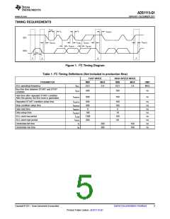
ADS1115-Q1
www.ti.com
SBAS563 –DECEMBER 2011
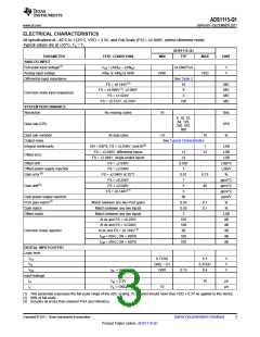
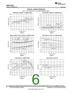
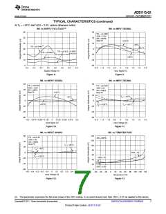
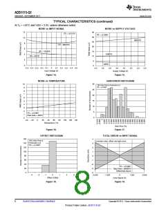
ELECTRICAL CHARACTERISTICS
All specifications at –40°C to +125°C, VDD = 3.3V, and Full-Scale (FS) = ±2.048V, unless otherwise noted.
Typical values are at +25°C, TA = TJ
ADS1115-Q1
PARAMETER
ANALOG INPUT
TEST CONDITIONS
MIN
TYP
MAX
UNIT
Full-scale input voltage(1)
VIN = (AINP) – (AINN)
±4.096/PGA
V
V
Analog input voltage
AINP or AINN to GND
GND
VDD
Differential input impedance
See Table 2
FS = ±6.144V(1)
FS = ±4.096V(1), ±2.048V
FS = ±1.024V
10
6
MΩ
MΩ
MΩ
MΩ
Common-mode input impedance
3
FS = ±0.512V, ±0.256V
100
SYSTEM PERFORMANCE
Resolution
No missing codes
16
Bits
SPS
%
8, 16, 32,
64, 128,
250, 475,
860
Data rate (DR)
Data rate variation
Output noise
All data rates
–10
10
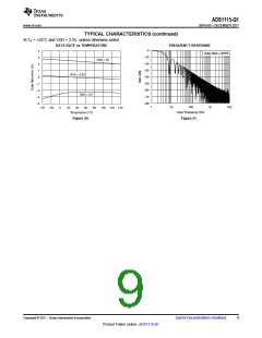
See Typical Characteristics
Integral nonlinearity
DR = 8SPS, FS = ±2.048V, best fit(2)
FS = ±2.048V, differential inputs
FS = ±2.048V, single-ended inputs
FS = ±2.048V
1
LSB
LSB
LSB
LSB/°C
LSB/V
%
±1
±3
±3
Offset error
Offset drift
0.005
1
Offset power-supply rejection
Gain error(3)
FS = ±2.048V
FS = ±2.048V at 25°C
FS = ±0.256V
0.01
7
0.15
40
ppm/°C
ppm/°C
ppm/°C
ppm/V
%
Gain drift(3)
FS = ±2.048V
FS = ±6.144V(1)
5
5
Gain power-supply rejection
PGA gain match(3)
Gain match
80
Match between any two PGA gains
Match between any two inputs
Match between any two inputs
At dc and FS = ±0.256V
0.02
0.05
3
0.1
0.1
%
Offset match
LSB
dB
105
100
90
At dc and FS = ±2.048V
At dc and FS = ±6.144V(1)
dB
Common-mode rejection
dB
fCM = 60Hz, DR = 8SPS
105
105
dB
fCM = 50Hz, DR = 8SPS
dB
DIGITAL INPUT/OUTPUT
Logic level
VIH
0.7VDD
GND – 0.5
GND
5.5
0.3VDD
0.4
V
V
V
VIL
VOL
IOL = 3mA
0.15
Input leakage
IH
IL
VIH = 5.5V
VIL = GND
10
μA
μA
10
(1) This parameter expresses the full-scale range of the ADC scaling. In no event should more than VDD + 0.3V be applied to this device.
(2) 99% of full-scale.
(3) Includes all errors from onboard PGA and reference.
Copyright © 2011, Texas Instruments Incorporated
Submit Documentation Feedback
3
Product Folder Link(s) :ADS1115-Q1

 TI [ TEXAS INSTRUMENTS ]