U211B2/ B3
Electrical Characteristics
–V = 13.0 V, T
= 25°C, reference point Pin 2, unless otherwise specified
S
amb
Parameters
Supply voltage for mains op-
eration
Test Conditions / Pins
Pin 3
Symbol
Min.
13.0
Typ.
Max.
V
Limit
Unit
V
–V
S
Supply voltage limitation
–I = 4 mA
–I = 30 mA
S
Pin 3
–V
–V
14.6
14.7
16.6
16.8
V
S
S
S
DC current requirement
Reference voltage source
–V = 13.0 V
Pin 3
Pin 16
I
–V
1.2
8.6
8.3
2.5
8.9
3.0
9.2
9.1
mA
V
S
S
–I = 10 A
L
Ref
–I = 5 mA
L
Temperature coefficient
Voltage monitoring
Turn-on threshold
Pin 16 –TC
0.5
mV/K
VRef
Pin 3 –V
11.2
9.9
13.0
10.9
V
V
SON
Turn-off threshold
Pin 3 –V
SOFF
Phase control currents
Synchronization current
Pin 1
0.35
0.35
1.4
2.0
2.0
1.8
mA
V
I
syncI
I
Pin 17
syncV
Voltage limitation
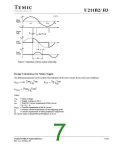
Reference ramp, figure 7
Charge current
1.6
I = 5 mA Pins 1 and 17
V
I
L
I = f (R );
7
6
R = 50 k to 1 M
Pin 7
Pins 6 and 3
Pin 6 TC
I
1
1.06
20
1.13
0.5
A
V
mV/K
6
7
R -reference voltage
Temperature coefficient
Pulse output, figure 18
Output pulse current
Reverse current
≥
°C
V
1.18
Ref
V Ref
Pin 4
= 0, V = 1.2 V
R
GT
I
o
100
155
0.01
80
190
3.0
mA
A
s
GT
I
or
Output pulse width
Amplifier
Cϕ = 10 nF
t
p
Common mode signal range
Input bias current
Input offset voltage
Output current
Pins 10 and 11
Pin 11
Pins 10 and 11
Pin 12
V ,
V
–1
1
V
A
mV
A
10 11
16
I
0.01
10
110
120
IO
V
10
–I
75
88
145
165
O
+I
O
Short circuit forward,
transmittance
Pulse blocking, tacho-monitoring
Logic-on
Logic-off
Input current
Figure 14
I
= f(V
)
Pin 12
Pin 18
Y
f
1000
A/V
V
12
10 -11
–V
3.7
1.5
1.25
0.3
TON
–V
1.0
1
TOFF
V
18
V
18
= V
= V
= 1.25 V
I
A
k
TOFF
16
I
14.5
1.5
Output resistance
R
O
6
10
TELEFUNKEN Semiconductors
9 (20)
Rev. A1, 29-May-96

 TEMIC [ TEMIC SEMICONDUCTORS ]