U211B2/ B3
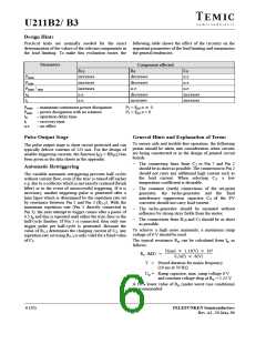
Absolute Maximum Ratings
Reference point Pin 2, unless otherwise specified
Parameters
Symbol
–I
Value
30
Unit
mA
Current requirement
Pin 3
S
–i
s
100
t ≤ 10 s
Synchronization current
Pin 1
Pin 17
Pin 1
I
5
5
35
35
mA
syncI
I
syncV
t
t
10 s
10 s
±i
I
±i
I
Pin 17
f/V converter
Pin 8
Input current
I
3
mA
I
±i
13
t
t
10 s
10 s
I
Load limiting
Pin 14
Limiting current, neg. half wave
I
5
35
1
mA
V
I
Input voltage
Pin 14
Pin 15
±V
i
–V
V
to 0
I
16
Phase control
Input voltage
Input current
Pin 12
Pin 12
Pin 6
–V
0 to 7
500
1
V
A
mA
I
±I
I
–I
I
Soft-start
Input voltage
Pulse output
Reverse voltage
Pulse blocking
Input voltage
Amplifier
Pin 13
Pin 4
–V
V
to 0
V
V
V
V
I
16
V
R
V to 5
S
Pin 18
–V
V
16
to 0
I
Input voltage
Pin 9 open
Pin 11
Pin 10
V
I
0 to V
S
–V
V
16
to 0
I
Reference voltage source
Output current
Storage temperature range
Junction temperature
Pin 16
I
7.5
–40 to +125
125
mA
°C
°C
o
T
stg
T
j
Ambient temperature range
T
amb
–10 to +100
°C
Thermal Resistance
Parameters
Symbol
Maximum
Unit
K/W
Junction ambient
DIP18
SO16 on p.c.
SO16 on ceramic
R
thJA
120
180
100
8 (20)
TELEFUNKEN Semiconductors
Rev. A1, 29-May-96

 TEMIC [ TEMIC SEMICONDUCTORS ]