U211B2/ B3
Parameters
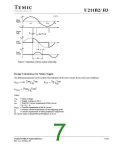
Frequency to voltage converter
Input bias current
Test Conditions / Pins
Symbol
Min.
Typ.
0.6
Max.
2
Unit
A
Pin 8
I
IB
Input voltage limitation
Figure 13
I = –1 mA
–V
+V
660
7.25
750
8.05
mV
V
I
I
I = +1 mA
I
I
Turn-on threshold
Turn-off threshold
Charge amplifier
Discharge current
–V
100
50
150
mV
mV
TON
–V
20
TOFF
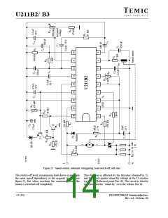
Figure 2
C = 1 nF,
Pin 9
I
0.5
mA
V
5
dis
Charge transfer voltage
Charge transfer gain
Conversion factor
Pins 9 to 16
Pins 9 and 10
V
G
i
6.50
7.5
6.70
8.3
6.90
9.0
ch
I /I
10
9
Figure 2
C = 1 nF, R = 100 k
K
5.5
0-6
1
mV/Hz
5
6
Output operating range
Linearity
Pins 10 to 16
V
O
V
%
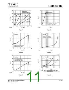
Soft-start, figures 8, 9, 10, 11, 12 f/v-converter non-active
Starting current
Final current
V
13
V
13
= V V = V Pin 13
I
20
50
45
85
55
130
A
16,
8
2
O
= 0.5
Pin 13
f/v-converter active
Starting current
Final current
Discharge current
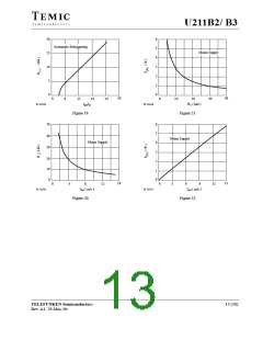
Automatic retriggering, figure 19
V
V
= V
= 0.5
Pin 13
I
I
2
30
0.5
4
55
3
7
80
10
A
A
mA
13
16
O
O
13
Restart pulse
Pin 13
Pin 5
Repetition rate
R
5-3
R
5-3
= 0
= 15 k
t
pp
3
4.5
20
6
t
p
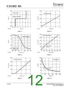
Load limiting, figures 15, 16, 17
Pin 14
Operating voltage range
Offset current
Pin 14
Pin 14
V
–1.0
5
1.0
12
V
I
V
V
= V
= V via 1 k
I
10
14
16
O
A
2
Pin 15–16
Pin 14
= 300 mV Pin 15–16
Pin 15–16
0.1
90
1.0
120
140
7.7
Input current
Output current
Overload ON
V
V
= 4.5 V
I
60
110
7.05
10
I
I
14
O
V
7.4
V
TON
10 (20)
TELEFUNKEN Semiconductors
Rev. A1, 29-May-96

 TEMIC [ TEMIC SEMICONDUCTORS ]