AN1008
Application Notes
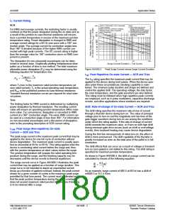
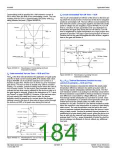
Commutating dv/dt is specified for a half sinewave current at
60 Hz which fixes the di/dt of the commutating current. The com-
mutating di/dt for 50 Hz is approximately 20% lower while IRMS
rating remains the same. (Figure AN1008.4)
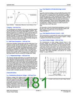
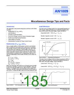
tq: Circuit-commutated Turn-off Time — SCR
The circuit-commutated turn-off time of the device is the time dur-
ing which the circuit provides reverse bias to the device (negative
anode) to commutate it off. The turn-off time occurs between the
time when the anode current goes negative and when the anode
positive voltage may be reapplied. (Figure AN1008.14) Turn-off
time is a function of many parameters and very dependent on
temperature and gate bias during the turn-off interval. Turn-off
time is lengthened for higher temperature so a high junction tem-
perature is specified. The gate is open during the turn-off interval.
Positive bias on the gate will lengthen the turn-off time; negative
bias on the gate will shorten it.
E
M
E
SOURCE
TIME
IG
IT
di/dt
ITRM
I
di/dt
TM
(di/dt)
C
50%
I
Off-State Leakage
Off-State Voltage
TM
I
I
D
50%
i
Reverse Current
RM
R
t
rr
Voltage across Triac
V
D
t
10%
63%
DRM
q
V
dv/dt
T
V
(dv/dt)
C
t
1
Figure AN1008.12 Waveshapes of Commutating dv/dt and
Associated Conditions
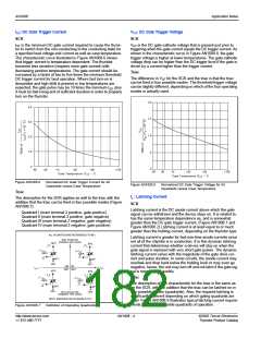
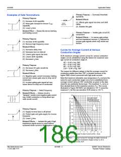
tgt: Gate-controlled Turn-on Time — SCR and Triac
Figure AN1008.14 Waveshapes of t Rating Test and
q
Associated Conditions
The tgt is the time interval between the application of a gate pulse
and the on-state current reaching 90% of its steady-state value.
(Figure AN1008.13) As would be expected, turn-on time is a
function of gate drive. Shorter turn-on times occur for increased
gate drives. This turn-on time is actually only valid for resistive
loading. For example, inductive loading would restrict the rate-of-
rise of anode current. For this reason, this parameter does not
indicate the time that must be allowed for the device to stay on if
the gate signal is removed. (Refer to the description of “IL: Latch-
ing Current” on page AN1008-4.) However, if the load was resis-
tive and equal to the rated load current value, the device
R
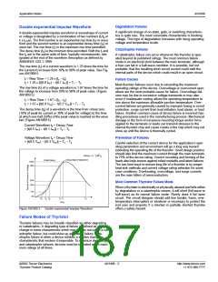
θJC, RθJA: Thermal Resistance (Junction-to-case,
Junction-to-ambient) — SCR and Triac
The thermal-resistance characteristic defines the steady-state
temperature difference between two points at a given rate of
heat-energy transfer (dissipation) between the points. The ther-
mal-resistance system is an analog to an electrical circuit where
thermal resistance is equivalent to electrical resistance, tempera-
ture difference is equivalent to voltage difference, and rate of
heat-energy transfer (dissipation) is equivalent to current. Dissi-
pation is represented by a constant current generator since gen-
erated heat must flow (steady-state) no matter what the
resistance in its path. Junction-to-case thermal resistance estab-
lishes the maximum case temperature at maximum rated steady-
state current. The case temperature must be held to the maxi-
mum at maximum ambient temperature when the device is oper-
ating at rated current. Junction-to-ambient thermal resistance is
established at a lower steady-state current, where the device is in
free air with only the external heat sinking offered by the device
package itself. For RθJA, power dissipation is limited by what the
device package can dissipate in free air without any additional
heat sink:
definitely would be operating at a current above the dynamic
latching current in the turn-on time interval since current through
the device is at 90% of its peak value during this interval.
90%
Off-state Voltage
10%
90%
On-state Current
10%
Delay
Time
Rise
Time
T
P
T
C
–
J
RθJC = ---------------------
Gate
Turn-on
(AV)
Trigger
Pulse
Time
T
P
T
–
J
A
50%
50%
RθJA = --------------------
10%
(AV)
Gate Pulse Width
Figure AN1008.13 Waveshapes for Turn-on Time and
Associated Conditions
http://www.teccor.com
+1 972-580-7777
AN1008 - 6
©2002 Teccor Electronics
Thyristor Product Catalog

 TECCOR [ TECCOR ELECTRONICS ]