ICM-20690
1 INTRODUCTION
1.1 PURPOSE AND SCOPE
This document is a product specification, providing a description, specifications, and design related information on the ICM-20690
Dual-Interface MotionTracking device. The device is housed in a small 2.5x3x0.91 mm 14-pin LGA package.
1.2 PRODUCT OVERVIEW
The ICM-20690 is a 6-axis MotionTracking device with a main Interface for UI and an Auxiliary interface configurable as SPI slave for
Optical Image Stabilization (OIS) applications or as I2C Master to support other sensors such as a compass or pressure sensor. It
combines a 3-axis gyroscope, and a 3-axis accelerometer in a small 2.5x3x0.91 mm (14-pin LGA) package. The device supports
independent data paths for UI and OIS, with independent control for full-scale range (FSR), output data rate (ODR).
ICM-20690 also features a 1K-byte FIFO that can lower the traffic on the serial bus interface, and reduce power consumption by
allowing the system processor to burst read sensor data and then go into a low-power mode. ICM-20690, with its 6-axis integration,
enables manufacturers to eliminate the costly and complex selection, qualification, and system level integration of discrete devices,
guaranteeing optimal motion performance for consumers.
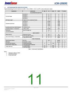
The gyroscope and accelerometer support the following independently programmable full-scale range settings:
Signal Path
UI Path
Gyroscope
Accelerometer
±31.25, ±62.5, ±125, ±250, ±500,
±1000, and ±2000 degrees/sec
±31.25, ±62.5, ±125, ±250, ±500,
±1000, and ±2000 degrees/sec
±2, ±4, ±8, ±16g
OIS Path
±1, ±2, ±4, ±8g
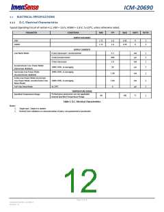
Other industry-leading features include on-chip 16-bit ADCs, programmable digital filters, an embedded temperature sensor, and
programmable interrupts. The device features I2C and SPI serial interfaces, a VDD operating range of 1.71 V to 3.45 V, and a separate
digital IO supply, VDDIO from 1.71 V to 3.45 V.
The host interface can be configured to support SPI slave or I2C slave modes. The SPI interface supports speeds up to 10 MHz and
the I2C interface supports speeds up to 400 kHz. A secondary interface can be configured to support SPI slave mode (3-wire) for
interfacing to OIS controllers, or I2C master mode for interfacing to external sensors. The SPI interface supports speeds up to
20 MHz and the I2C interface supports speeds up to 400 kHz.
By leveraging its patented and volume-proven CMOS-MEMS fabrication platform, which integrates MEMS wafers with companion
CMOS electronics through wafer-level bonding, InvenSense has driven the package size down to a footprint and thickness of
2.5x3x0.91 mm (14-pin LGA), to provide a very small yet high performance low cost package. The device provides high robustness
by supporting 20,000g shock reliability.
1.3 APPLICATIONS
Smartphones and Tablets
Head Mounted Displays
Wearable Sensors
Page 8 of 76
Document Number: DS-000178
Revision: 1.0

 TDK [ TDK ELECTRONICS ]