ICM-20690
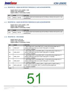
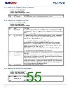
12.27 REGISTER 44 – I2C SLAVE 2 REGISTER ADDRESS
Register Name: I2C_SLV2_REG
Register Type: READ/WRITE
Register Address: 44 (Decimal); 2C (Hex)
BIT
[7:0]
NAME
I2C_SLV2_REG
FUNCTION
I2C slave 2 register address from where to begin data transfer.
12.28 REGISTER 45 – I2C SLAVE 2 CONTROL
Register Name: I2C_SLV2_CTRL
Register Type: READ/WRITE
Register Address: 45 (Decimal); 2D (Hex)
BIT
NAME
FUNCTION
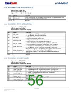
[7]
I2C_SLV2_EN
1 – Enable reading data from this slave at the sample rate and storing data at the
first available EXT_SENS_DATA register, which is always EXT_SENS_DATA_00 for I2C
slave 0.
0 – Function is disabled for this slave.
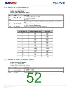
[6]
I2C_SLV2_BYTE_S
W
1 – Swap bytes when reading both the low and high byte of a word. Note there is
nothing to swap after reading the first byte if I2C_SLV2_REG[0] = 1, or if the last
byte read has a register address lsb = 0.
For example, if I2C_SLV2_REG = 0x1, and I2C_SLV2_LENG = 0x4:
1) The first byte read from address 0x1 will be stored at EXT_SENS_DATA_00,
2) The second and third bytes will be read and swapped, so the data read from
address 0x2 will be stored at EXT_SENS_DATA_02, and the data read from address
0x3 will be stored at EXT_SENS_DATA_01,
3) The last byte read from address 0x4 will be stored at EXT_SENS_DATA_03
0 – No swapping occurs; bytes are written in the order read.
[5]
[4]
I2C_SLV2_REG_DIS When set, the transaction does not write a register value, it will only read data, or
write data.
I2C_SLV2_GRP
External sensor data typically comes in as groups of two bytes. This bit is used to
determine if the groups are from the slave’s register address 0 and 1, 2 and 3, etc..,
or if the groups are address 1 and 2, 3 and 4, etc..
0 indicates slave register addresses 0 and 1 are grouped together (odd numbered
register ends the group). 1 indicates slave register addresses 1 and 2 are grouped
together (even numbered register ends the group). This allows byte swapping of
registers that are grouped starting at any address.
3:0
I2C_SLV2_LENG
Number of bytes to be read from I2C slave 2.
12.29 REGISTER 46 – FSYNC ODR DELAY ENABLE
Register Name: ODR_DELAY_EN
Register Type: READ/WRITE
Register Address: 46 (Decimal); 2E (Hex)
BIT
[7]
NAME
FUNCTION
1 – Enables FSYNC ODR delay counter.
0 – Function is disabled.
Reserved
ODR_DELAY_EN
-
[6:0]
Page 55 of 76
Document Number: DS-000178
Revision: 1.0

 TDK [ TDK ELECTRONICS ]