ICM-20690
12.9 REGISTER 25 – SAMPLE RATE DIVIDER
Register Name: SMPLRT_DIV
Register Type: READ/WRITE
Register Address: 25 (Decimal); 19 (Hex)
BIT
NAME
FUNCTION
[7:0]
SMPLRT_DIV[7:0]
Divides the internal sample rate (see register CONFIG) to generate the
sample rate that controls sensor data output rate, FIFO sample rate.
NOTE: This register is only effective when FCHOICE_B register bits are
2’b00, and (0 < DLPF_CFG < 7).
This is the update rate of the sensor register:
SAMPLE_RATE = INTERNAL_SAMPLE_RATE / (1 + SMPLRT_DIV)
Where INTERNAL_SAMPLE_RATE = 1kHz
SMPLRT_DIV values of 0 and 1 are not supported in low-power mode.
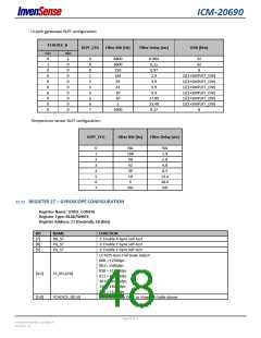
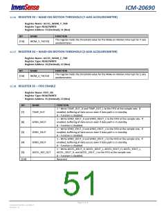
12.10 REGISTER 26 – CONFIGURATION
Register Name: CONFIG
Register Type: READ/WRITE
Register Address: 26 (Decimal); 1A (Hex)
BIT
[7]
[6]
NAME
FIFO_MODE
FUNCTION
-
Default configuration value is 1. User should set it to 0.
When set to ‘1’, when the FIFO is full, additional writes will not be written to FIFO.
When set to ‘0’, when the FIFO is full, additional writes will be written to the FIFO,
replacing the oldest data.
[5:3] EXT_SYNC_SET[2:0]
Enables the FSYNC pin data to be sampled.
EXT_SYNC_SET
FSYNC bit location
function disabled
TEMP_OUT_L[0]
GYRO_XOUT_L[0]
GYRO_YOUT_L[0]
GYRO_ZOUT_L[0]
ACCEL_XOUT_L[0]
ACCEL_YOUT_L[0]
ACCEL_ZOUT_L[0]
0
1
2
3
4
5
6
7
FSYNC will be latched to capture short strobes. This will be done such that if FSYNC
toggles, the latched value toggles, but won’t toggle again until the new latched value
is captured by the sample rate strobe.
[2:0] DLPF_CFG[2:0]
For the DLPF to be used, FCHOICE_B[1:0] is 2’b00.
See the tables below.
The DLPF is configured by DLPF_CFG, when FCHOICE_B [1:0] = 2b’00. The gyroscope and temperature sensor are filtered
according to the value of DLPF_CFG and FCHOICE_B as shown in the table below.
Page 47 of 76
Document Number: DS-000178
Revision: 1.0

 TDK [ TDK ELECTRONICS ]