SyncMOS Technologies International, Inc.
SM89T16R1
8-Bits Micro-controller
With 64KB Flash ROM & 1KB RAM & Two UART & RTC & ADC & PWM embedded
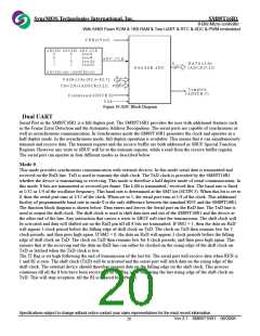
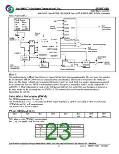
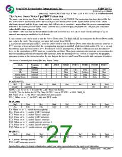
Serial Port Mode 2:
Clock Source
TB8
D8
Mode
1/4
Input
osc/2
osc/32
STOP
PARIN
START
LOAD
CLOCK
RxD
Internal
1/64
P3.0 Alternate
Input function
SOUT
Data Bus
1/1024 osc/512
Write to
SBUF
1/2
SMOD=
TX START
TX CLOCK
TX SHIFT
0
1
Transmit Shift Register
(SMOD 1)
1/16
1/16
TI
RI
Serial Port Interrupt
TxD
SHIFT CLOCK
P3.1 Alternate
Input function
LOAD SBUF
RX SHIFT
SAMPLE
RX CLOCK
READ SBUF
SBUF
1- To-0
RX START
Detector
CLOCK
Internal
SBUF
RB8
PAROUT
D8
Data Bus
Bit
RxD
Detector
SIN
P3.0 Alternate
Input function
Receive Shift Register
Mode 3
This mode is similar to Mode 2 in all respects; expect that the baud rate is programmable. The user must first initialize
the Serial related SFR SCON before any communication can take place. This involves selection of the Mode and
Baud rate. The Timer 1 should also be initialized if modes 1 and 3 are used. In all four modes, transmission is started
by any instruction that uses SBUF as a destination register. Reception is initiated in Mode 0 by the condition RI = 0
and REN = 0. This will generate a clock on the TxD pin and shift in 8 bits on the RxD pin. Reception is initiated in
the other modes by the incoming start bit if REN = 1. The external device will start the communication by
transmitting the start bit.
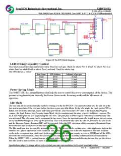
Pulse Width Modulation (PWM)
The PWM output pins are P1.4 and P1.5.
The PWM clock is {Fosc/ (2xDivider)}, the PWM output frequency is {(PWM clock)/32} at 5 bits resolution and
{(PWM clock)/256} at 8 bits resolution.
The PWM SFR is shown as below:
PWMC ($D3H and $D4H)
Bit7
Bit6
Bit5
Bit4
Bit3
Bit2
PBS
Bit1
PFS1
Bit0
PFS0
PBS: when set, the PWM is 5 bits resolution.
PFS [1:0]: The PWM clock divider select.
PFS1
PFS0
PWM clock divider select
0
0
1
1
0
1
0
1
1
2
4
8
Specifications subject to change without notice contact your sales representatives for the most recent information.
Ver 2.1 SM89T16R1 08/2006
23

 SYNCMOS [ SYNCMOS TECHNOLOGIES,INC ]