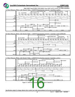
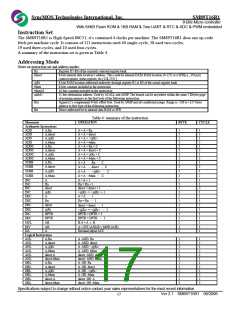
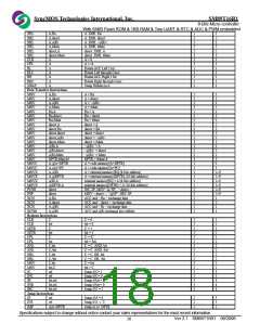
SyncMOS Technologies International, Inc.
SM89T16R1
8-Bits Micro-controller
With 64KB Flash ROM & 1KB RAM & Two UART & RTC & ADC & PWM embedded
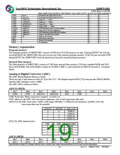
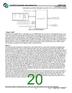
V D D (= V re f)
A D C S S 1 A D C S S 0 A D C _ C L K
0
0
1
1
0
1
0
1
F o sc /4
F o sc /8
F o sc /1 6
F o sc /3 2
A D C _ C L K
D A T A < 5 :0 >
{ A D C D [7 :2 ]}
6
6 -b it S A R A D C
A D C S S [1 :0 ]= { A D S C R [5 :4 ]}
4
V A IN < 3 :0 > { P 2 .4 ~ P 2 .7 }
C H < 2 :0 > { A D S C R [3 :2 ]}
3
C o m p le te
{ A D S C R .7 }
C o n tin u o u s{ A D S C R .6 }
V S S
Figure 16 ADC Block Diagram
Dual UART
Serial Port in the SM89T16R1 is a full duplex port. The SM89T16R1 provides the user with additional features such
as the Frame Error Detection and the Automatic Address Recognition. The serial ports are capable of synchronous as
well as asynchronous communication. In Synchronous mode the SM89T16R1 generates the clock and operates in a
half duplex mode. In the asynchronous mode, full duplex operation is available. This means that it can simultaneously
transmit and receive data. The transmit register and the receive buffer are both addressed as SBUF Special Function
Register. However any write to SBUF will be to the transmit register, while a read from the receive buffer register.
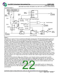
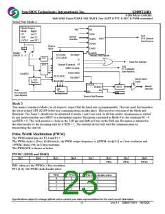
The serial port can operate in four different modes as described below.
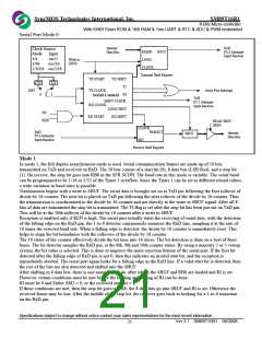
Mode 0
This mode provides synchronous communication with external devices. In this mode serial data is transmitted and
received on the RxD line. TxD is used to transmit the shift clock. The TxD clock is provided by the SM89T16R1
whether the device is transmitting or receiving. This mode is therefore a half duplex mode of serial communication. In
this mode, 8 bits are transmitted or received per frame. The LSB is transmitted / received first. The baud rate is fixed
at 1/12 or 1/4 of the oscillator frequency. This baud rate is determined at the SM2 bit (SCON.5). When this bit is set to
0, then the serial port runs at 1/12 of the clock. When set to 1, the serial port runs at 1/4 of the clock. This additional
facility of programmable baud rate in mode 0 is the only difference between the standard 8051 and the SM89T16R1.
The function block diagram is shown below. Data enters and leaves the Serial port on the RxD line. The TxD line is
used to output the shift clock. The shift clock is used to shift data into and out of the SM89T16R1 and the device at
the other end of the line. Any instruction that causes a write to SBUF will start the transmission. The shift clock will
be activated and data will shifted out on the RxD pin till all 8 bits are transmitted. If SM2 = 1, then the data on RxD
will appear 1 clock period before the falling edge of shift clock on TxD. The clock on TxD then remains low for 2
clock periods, and then goes high again. If SM2 = 0, the data on RxD will appear 3 clock periods before the falling
edge of shift clock on TxD. The clock on TxD then remains low for 6 clock periods, and then goes high again. This
ensures that at the receiving end the data on RxD line can either be clocked on the rising edge of the shift clock on
TxD or latched when the TxD clock is low.
The TI flag is set high following the end of transmission of the last bit. The serial port will receive data when REN is
1 and RI is zero. The shift clock (TxD) will be activated and the serial port will latch data on the rising edge of the
shift clock. The external device should therefore present data on the falling edge on the shift clock. This process
continues till all the 8 bits have been received. The RI flag is set following the last rising edge of the shift clock on
TxD. This will stop reception, till the RI is cleared by software.
Specifications subject to change without notice contact your sales representatives for the most recent information.
Ver 2.1 SM89T16R1 08/2006
20

 SYNCMOS [ SYNCMOS TECHNOLOGIES,INC ]