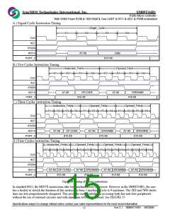
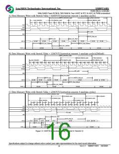
SyncMOS Technologies International, Inc.
SM89T16R1
8-Bits Micro-controller
With 64KB Flash ROM & 1KB RAM & Two UART & RTC & ADC & PWM embedded
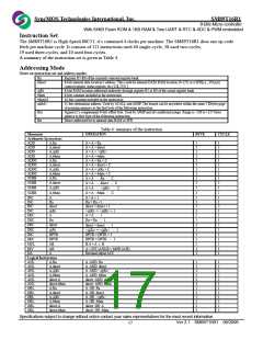
DJNZ
DJNZ
CJNE
Ri,rel
Decrement and jump if Rn not zero
Decrement and jump if direct not zero
Jump if A ≠ < direct >
2
3
3
3
4
4
Direct,rel
A,direct,rel
CJNE
CJNE
CJNE
A,#data,rel
@Ri,#data,rel
Ri,#data,rel
Address11
Address11
Address16
Address16
rel
3
3
3
2
2
3
3
2
1
1
1
4
4
4
3
3
4
4
3
3
3
1
Jump if A ≠ < #data >
Jump if Rn ≠ < #data >
Jump if @Ri ≠ < #data >
Call Subroutine only at 2k bytes Address
Jump only At 2k bytes addressing
Call Subroutine in max 64K bytes Address
Jump to max 64K bytes Address
Jump on at 256 bytes
ACALL
AJMP
LCALL
LJMP
SJMP
RET
Return from subroutine
RETI
NOP
Return from interrupt
No Operation
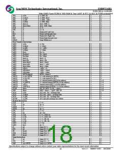
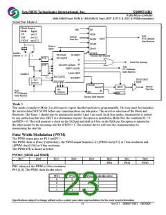
Memory organization
Program memory
The program memory of SM89T16R1 consists of 64K bytes FLASH memory on chip. If during RESET, the /EA pin
was held HIGH, the SM89T16R1 does not execute out of the internal program memory. If the /EA pin was held LOW
during RESET the SM89T16R1 fetch all instructions from the external program memory.
Internal Data memory
The Data memory of SM89T16R1 consists of 1280 bytes internal data memory (256 bytes standard RAM and 1024
bytes AUX-RAM). The AUX-RAM is enable by SCONF.1 ($BF.1), and read/write by MOVX (Stretch=0, 2 machine
fixed)
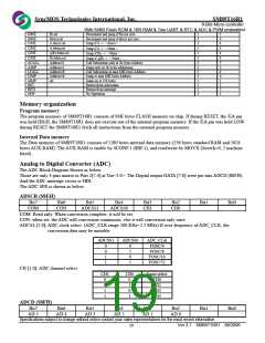
Analog to Digital Converter (ADC)
The ADC Block Diagram Shown as below:
Those are only 4 pins mirror to Port 2[7:4] at Vin<3:0>. The Digital output DATA [7:0] were put into ADCD ($8FH).
And the ADC interrupt vector is 4BH.
The ADC SFR is shown as below:
ADSCR ($8EH)
Bit7
Bit6
CON
Bit5
ADCSS1
Bit4
ADCSS0
Bit3
CH1
Bit2
CH0
Bit1
Bit0
COM
COM: Read only. When conversion complete, it will be set.
CON: when set, the ADC will conversion continuous, else it will conversion only once.
ADCSS [1:0]: ADC clock select. (ADC_CLK range 500 KHz~2.5 MHz).If over frequency of ADC_CLK, the
conversion data may be unstable.
ADCSS1
ADCSS0
ADC_CLK
FOSC/4
0
0
1
1
0
1
0
1
FOSC/8
FOSC/16
FOSC/32
CH [1:0]: ADC channel select.
CH1
CH0
Input select
CH0
0
0
1
1
0
1
0
1
CH1
CH2
CH3
ADCD ($8FH)
Bit7
Bit6
AD.4
Bit5
AD.3
Bit4
AD.2
Bit3
AD.1
Bit2
AD.0
Bit1
Bit0
AD.5
Specifications subject to change without notice contact your sales representatives for the most recent information.
Ver 2.1 SM89T16R1 08/2006
19

 SYNCMOS [ SYNCMOS TECHNOLOGIES,INC ]