SMM151/152
APPLICATIONS INFORMATION
DEVICE OPERATION
the actual converter output voltage. The voltage on the
TRIM output will continue increasing or decreasing
until the converter’s output voltage equals the target
margin voltage. This voltage adjustment allows the
SMM151 and SMM152 to control the margined output
voltage of the power supply converter to within ±1.0%
in an open-loop manner.
The converter is held at the margin voltage until the
SMM151 receives an I2C command or the respective
MUP/MDN pin is de-asserted. When not margining,
the TRIM pin on the SMM151/152 is in a high
impedance state. The voltage on the TRIM pin is
buffered and applied to the ADC at the beginning of a
margin cycle to ensure the converter is margined from
its nominal setpoint. This allows a smooth transition
from the converter’s nominal voltage to the
SMM151/152 controlling that margin voltage to the
margin target setting. After margining high, low or
nominal, issuing a margin Off command will cause the
trim pin to go high impedance. The part margin time
from Off to High or Off to Low is specified as a typical
according to the equation:
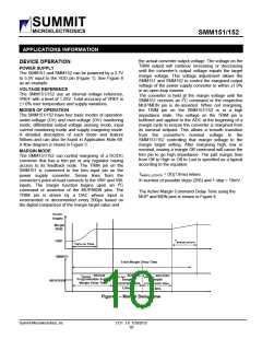
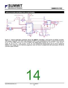
POWER SUPPLY
The SMM151 and SMM152 can be powered by a 2.7V
to 5.5V input to the VDD pin (Figure 1). See Figure 6
as an example.
VOLTAGE REFERENCE
The SMM151/152 use an internal voltage reference,
VREF with a level of 1.25V. Total accuracy of VREF is
±1.0% over temperature and supply variations.
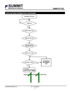
MODES OF OPERATION
The SMM151/152 have four basic modes of operation:
under-voltage (UV) and over-voltage (OV) monitoring
mode, differential output voltage sensing mode, input
current monitoring mode and supply margining mode.
A detailed description of each mode and feature
follows and can also be found in Application Note 68.
A flow diagram is shown in Figure 5.
MARGIN MODE
The SMM151/152 can control margining of a DC/DC
converter that has a trim pin or any regulator having
access to its feedback node. The TRIM pin on the
SMM151 is connected to the trim input pin on the
power supply converter. Sense lines from the
converter’s point-of-load connects to the VM+ and VM-
inputs. The margin function begins upon an I2C
command or assertion of the MUP/MDN pins. The
TRIM pin is driven by a DAC whose input is
incremented or decremented every 200µs based on
the digital comparison of the margin target value and
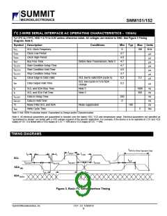
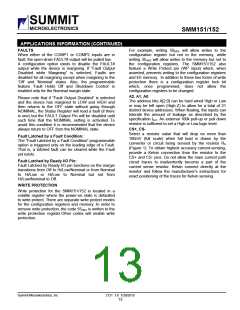
TMARG_UPDATE = (X)(1.8ms) where:
X=number of possible steps (256) and 1 step = 10mV
The Active Margin Command Delay Time using the
MUP and MDN pins is shown in Figure 4.
DC/DC
Supply
Margin
N/H/L
GND
TMARGIN_UPDATE
Turn on Time
SMM151
Total Margin Delay Time
tMARGIN - Internal
Programmable Active
Margin Delay Time
tADC_DAC ADC/DAC
Sample/
Conversion time
tADC_DAC ADC/DAC
Sample/
Conversion time
MPU/D/EN
1.8ms
1.8ms
Figure 4 – Margin Delay Time
Summit Microelectronics, Inc
2131 3.0 1/20/2010
10

 SUMMIT [ SUMMIT MICROELECTRONICS, INC. ]