SMM151/152
APPLICATIONS INFORMATION (CONTINUED)
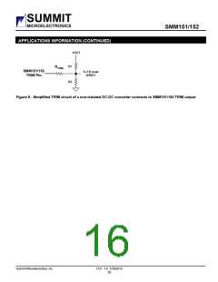
When measuring the margin delay time external to the
device, ADC sample time and Update Trim time (≅ 3.6
ms) must be added to the internally programmed delay
time as shown:
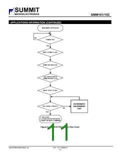
from bit 0 of registers 34h, 35h, 36h or 37h with 0=Low
and 1=High. Additionally, the I/Os have a command bit
that when written overrides the NV setting and sets the
pin either high or low. The I/Os also have status bits to
read the state of the pin as high or low. The
command/status register for each I/O is addressed
separately alleviating the need for the host controller to
remember the state of the other I/Os when writing
commands. More information can be found in
Application Note 69.
Spec
2.5 ms
5 ms
Actual measurement
6.1 ms
8.6 ms
10 ms
17.5 ms
13.6 ms
21.1 ms
MONITOR
STATUS REGISTER
The SMM151/152 monitor the COMP1 and COMP2
pins. COMP1 and COMP2 are high impedance inputs,
each connected internally to a comparator and
compared against the programmable internal reference
voltage. Each comparator can be independently
programmed to monitor for either an UV or an OV
event. The monitor level may be set externally with a
resistive voltage divider. The COMPx pins can be
connected to Vin, Vout or any voltage that needs to be
monitored. The internal comparators COMP1/2 are
compared to VREF, so the voltage dividers are set
above or below the programmed VREF level depending
on whether monitoring UV or OV. As an example, with
VREF set to 1.25V, to monitor an OV of 1.7V on
COMP1 and a UV of 1.3V on COMP2, the voltage
divider resistors are:
A status register exists for I2C polling of the status of
the COMP1 and COMP2 inputs. Two bits in this status
register reflect the current state of the inputs (1 = fault,
0 = no fault). Two additional bits show the state of the
inputs latched by one of two events programmed in the
configuration. More information can also be found in
Application Note 69. The first event option is the
FAULT# output going active. The second event option
is the READY pin going low. The READY pin is an I/O.
As an output, the READY output pin goes active when
the DC controlled voltages are at their set point. As an
input programmed to active high, it can be pulled low
externally and latch the state of the COMP inputs. This
second event option allows the state of the COMP
inputs on multiple devices to be latched at the same
time while a host monitors their FAULT# outputs.
For OV, RUpper = 1.37k, 1% RLower = 3.83k, 1%.
For UV, RUpper = 1.02k, 1% RLower = 25.5k, 1%.
MARGINING
The SMM151/152 have three additional control voltage
settings: margin high, margin nominal, and margin low.
The margin high and margin low settings can be as
much as ±15% of the nominal setting depending on the
converter manufacturer. The margin high and margin
low voltage settings can range from 0.3V to VDD
around the converters’ nominal output voltage setting
depending on the specified margin range of the DC-DC
converter. These settings are stored in the
configuration registers and are loaded as control
voltage settings by margin commands issued via the
I2C bus.
The margin command registers contain two bits that
decode the commands to margin high or margin low.
Once the SMM151/152 receive the command to margin
the supply voltage, it begins adjusting the supply
voltage to move toward the desired setting. When this
voltage setting is reached, a bit is set in the margin
status registers and the READY signal becomes active.
Note: Configuration writes or reads of registers 00HEX to
03HEX should not be performed while the SMM151 or
SMM152 is margining.
The parts can be programmed to trigger the FAULT#
pin when either COMPx comparator has exceeded the
UV or OV setting. The READY and FAULT# outputs of
the SMM151/152 are active as long as the triggering
limit remains in a fault condition. The READY pin is a
programmable active high/low open drain output
indicates that VM+ - VM- is at its’ set point.
When programmed as an active high output, READY
can also be used as an input. When pulled low, it will
latch the state of the comparator inputs. When either of
the COMP1 or COMP2 inputs are in fault, the open-
drain FAULT# output will be pulled low. A configuration
option exists to disable the FAULT# output while the
device is in margining mode.
GENERAL-PURPOSE INPUTS/OUTPUTS
The GPIOs are open drain type outputs. The
pins should be pulled up externally to voltages ranging
from 2.0V to 12V. Each I/O has non-volatile (NV)
memory setting associated with it that determines the
power-on state of the pin. The status (High/Low) is read
Summit Microelectronics, Inc
2131 3.0 1/20/2010
12

 SUMMIT [ SUMMIT MICROELECTRONICS, INC. ]