SMM151/152
APPLICATIONS INFORMATION (CONTINUED)
READY
+VIN 2.7V- 5.5V
FAULT#
12VIN
MUP
VDD
R6
0.01, 1%
MDN
VDD
VDD
C1
0.01uF
C2
0.1uF
C3
10uF
U2
DC-DC SIE
+Vout
VDD
7
8
11
9
1
2
VOUT = 1.5V
+Vin
+Vin
Enable
+Vin
+Sense
4
3
C12
C Load
R7
R Load
-Vout
-Sense
Programming Supply
U1
C10
0.1uF
C11
0.01uF
25
24
MDN
MUP
19
12
14
Comp1
Comp2
VM+
DIODE
D1
1
28
J1
SCL
SDA
SMM151
1
2
4
6
8
Gnd
Gnd3
Rsrv5
+10V Rsrv8
+5V Rsrv10
SCL
SDA
MR
3
5
7
9
6
4
2
8
15
20
26
10
A0
A1
A2
WP#
VM-
Trim
R5
2.5k
10
I2C
R1
R3
R2
VREF
CAPM+
7
Gnd
C7
0.1uF
C6
0.22uF
13
CAPM-
3
92227
R4
NCNCNCNC
C4
0.47uF
C5
1uF
C8
0.01uF
C9
0.01uF
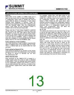
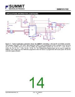
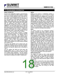
Figure 6 – Typical application schematic shows the SMM151 controlling a 12V in/1.5V out DC/DC converter.
This example, using the 1.25V VREF, also shows the COMP1/2 pins monitoring the DC/DC converter VOUT set to an
OV of 1.7V on COMP1 and a UV of 1.3V on COMP2, the voltage divider resistors are: For OV, R1 = 1.37k, 1% R3 =
3.83k, 1%, For UV, R2 = 1.02k, 1% R4 = 25.5k, 1%. The Programming Supply jumper can be used to supply the
SMM151 VDD voltage from the SMX3202 programmer when the device is programmed with board power off and the
controlled supply unloaded.
Summit Microelectronics, Inc
2131 3.0 1/20/2010
14

 SUMMIT [ SUMMIT MICROELECTRONICS, INC. ]