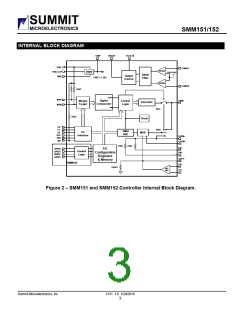
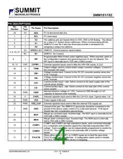
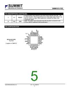
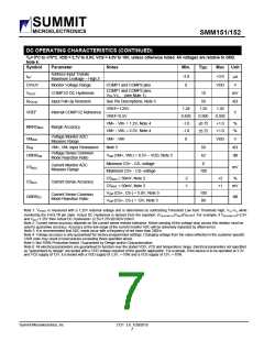
SMM151/152
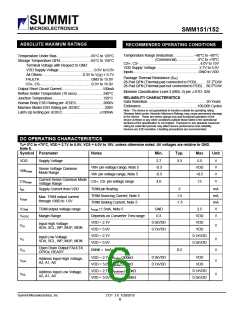
DC OPERATING CHARACTERISTICS (CONTINUED)
TA= 0°C to +70°C, VDD = 2.7V to 5.5V, VCS = 4.0V to 15V, unless otherwise noted. All voltages are relative to GND.
Note 6.
Symbol
Parameter
Notes
Min.
Typ.
Max
Unit
Address Input Tristate
Maximum Leakage – High Z
IAIT
-3.0
0
+3.0
VDD
μA
V
OV/UV
VHYST
RPull-Up
Monitor Voltage Range
COMP1/2 DC Hysteresis
Input Pull-Up Resistors
COMP1 and COMP2 pins
COMP1 and COMP2 pins,
VTH-VTL (see Note 1)
10
mV
kΩ
See Pin Descriptions, Note 5
VREF=1.25V
50
1.24
0.495
-1.0
1.25
1.26
0.505
+1.0
+1.0
VREF
Internal COMP1/2 Reference
Margin Accuracy
V
VREF=0.5V
0.500
±0.75
±0.75
VM+ - VM- = 1.2V, Note 4
VM+ - VM- = 2.5V, Note 4
%
%
MARGACC
-1.0
Voltage Monitor ADC
Measure Range
VMADC
RVM
VM+ - VM-
0
VDD
V
VM+, VM- Input Resistance
Note 5
50
62
kΩ
dB
Voltage Sense Common
Mode Rejection Ratio
CMRRVM
VCM (VM+, VM-) = 0.5V – VDD, Note 5
Minimum CS+ - CS- voltage
Maximum CS+ - CS- voltage
CSADC ≥ 50mV, Note 2
0
Current Monitor ADC
Measure Range
CSADC
mV
100
-2
-1
+2
+1
%
CSACC
Current Sense Accuracy
CSADC < 50mV, Note 2
mV
VCM (CS+, CS-) = 5.0V, Note 5
VCM (CS+, CS-) = 12V, Note 5
100
80
Current Sense Common
Mode Rejection Ratio
CMRRCS
dB
Note 1: VHYST is measured with a 1.25V external voltage and is determined by subtracting Threshold Low from Threshold High, VTH-VTL while
monitoring the FAULT# pin state. Actual DC Hysteresis is derived from the equation: (VIN(COMP1/2)/VREF)(VHYST). For example, if VIN(COMP1/2)/=2.5V
and VREF=1.25V then Actual DC Hysteresis= (2.5V/1.25V)(0.003V)=6mV.
Note 2: Current sense accuracy depends on the current sense resistor tolerance. Kelvin sensing of the voltage drop across this resistor must be
used to guarantee accuracy. Accuracy at the low range of the current monitor ADC will be adversely impacted by offset errors.
Note 3: It is recommended that ADC reads occur with a frequency of not more than 250Hz.
Note 4: Voltage accuracy is only guaranteed for factory-programmed settings. Changing voltage from the value reflected in the customer specific
CSIR code may result in inaccuracies exceeding those specified above.
Note 5: Not 100% Production tested. Guaranteed by Design and/or Characterization.
Note 6: All electrical parameters are guaranteed to function over the stated VDD, VCS and temperature range. Electrical parameters not specified
as "guaranteed by design" are tested with a VDD voltage required of the specific application. For example, if the device is to be operated at 3.3V
and VCS supply of 12V, it is tested with a VDD supply of 3.3V, +-10% and a VCS supply of 12V, +-10%.
Summit Microelectronics, Inc
2131 3.0 1/20/2010
7

 SUMMIT [ SUMMIT MICROELECTRONICS, INC. ]