SMD1102 / 1103 / 1113
DEVICE OPERATION
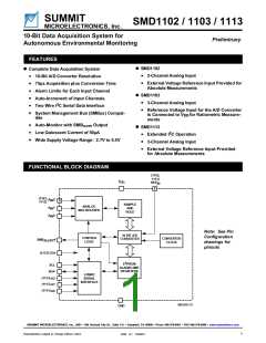
TheSMD1102,SMD1103andSMD1113DataAcquisition The next bit in the addressing sequence is the EEPROM/
Systems (DAS) are each comprised of: an analog input Conversion (E/C) bit; when set to zero the device is
multiplexer, sample-and-hold circuit, 10-Bit successive instructed to perform an A/D conversion, and when set to
approximation Analog-to-Digital (A/D) Converter, and logic one the EEPROM limit register will be addressed.
nonvolatile EEPROM memory to store upper and lower See Table 1A.
alarm-limits for each input channel. The user programs
The next two bits are the channel select bits. Auto-
thealarmlimitsviatheindustry-standardI2Cinterface. An
increment is enabled if the channel select bits are set to
SMBALERT# interrupt output signals if any of the analog
11BIN and the conversion bit is set to zero. In the auto-
inputs move outside these limits.
increment mode conversions are performed on succes-
sive channels, starting with channel 0. After channel 2 is
DAS Modes of Operation
converted (channel 1 on the SMD1102) the address will
wrap around to channel 0. See Table 1B.
The SMD1102/1103/1113 have four user-selectable
modes of operation. These modes are: a single conver-
sionofonechannel, successiveconversionsonthesame
The last bit is the Read/Monitor bit. When the bit is set
to logic one, data can be read from a conversion or from
channel, sequential conversions on all three channels, or
oneoftheEEPROMlimitregisters,dependingonthestate
oftheEEPROM/Conversionbit. Whenthebitislogiczero
autonomous conversions of the same or all channels.
either the auto-monitor mode is entered or the EEPROM
limitregisterisprogrammed,againdependingonthestate
of the EEPROM/Conversion bit. See Table 1C.
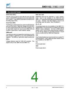
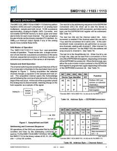
Sample-and-Hold Operation
ThechannelswitchingandsamplingarchitectureoftheA/
D’s comparator is illustrated in the equivalent input circuit
diagram in Figure 1. During acquisition the selected
channel charges a capacitor in the sample-and-hold cir-
DB7 DB6 DB5 DB4 DB3
Function
cuit. The acquisition interval spans the Acknowledge
periodfollowingthecommandbyteandendsontherising
edgeofthenextclock. Attheendoftheacquisitionphase
the analog input is disconnected, retaining charge on the
hold capacitor as a sample of the signal.
Device Type Identifier
E/C
Perform A/D con-
version on selected
channel(s)
A2
A1
A0
0
or
or
or
1
Address EEPROM
limit register
1
Buffer
1*
0*
0*
Sample
Analog In
& Hold
2033 Table01A
* Denotes SMD 1102 & SMD1103. Ax bits are for the SMD1113.
+
–
Table 1A. Address Byte — EEPROM/Conversion
DAC
DB7 DB6 DB5 DB4 DB2 DB1
Function
Device Type Identifier CH1 CH0
SAR
SDA
Channel 0
selected
0
0
1
1
0
1
0
1
2033 Fig01 2.0
Figure 1. Sample/Hold and SAR
A2 A1 A0
Channel 1
selected
or
or
or
1
Channel 2
selected
Addressing and Command Sequence
All operations of the DAS are preceded first by the start
condition and then by the addressing command se-
quence. FortheSMD1102&SMD1103thisis1001BIN. For
the SMD1113 it is the binary values of A2, A1, A0, and a
one — a four bit number.
1*
0*
0*
Auto-increment if
E/C = 0
2033 Table01B
* Denotes SMD 1102 & SMD1103. Ax bits are for the SMD1113.
Table 1B. Address Byte — Channel Select
SUMMIT MICROELECTRONICS, Inc.
2033 8.1 10/04/01
5

 SUMMIT [ SUMMIT MICROELECTRONICS, INC. ]