SMD1102 / 1103 / 1113
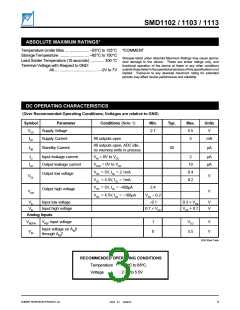
ABSOLUTE MAXIMUM RATINGS*
Temperature Under Bias ...................... –55°C to 125°C *COMMENT
Storage Temperature ........................... –65°C to 150°C
Stresses listed under Absolute Maximum Ratings may cause perma-
nent damage to the device. These are stress ratings only, and
functional operation of the device at these or any other conditions
outside those listed in the operational sections of this specification is not
implied. Exposure to any absolute maximum rating for extended
periods may affect device performance and reliability.
Lead Solder Temperature (10 seconds) ............. 300 °C
Terminal Voltage with Respect to GND:
All......................................... –2V to 7V
DC OPERATING CHARACTERISTICS
(Over Recommended Operating Conditions; Voltages are relative to GND)
Symbol
VCC
Parameter
Supply Voltage
Conditions (Note 1)
Min.
Typ.
Max.
5.5
3
Units
V
2.7
ICC
Supply Current
Standby Current
All outputs open
mA
All outputs open, ADC idle,
no memory write in process
ISB
50
µA
ILI
Input leakage current
Output leakage current
VIN = 0V to VCC
2
µA
µA
ILO
VOUT = 0V to VCC
10
0.4
0.2
VCC = 5V, IOL = 2.1mA
VCC < 4.5V, IOL = 1mA
VCC = 5V, IOL = –400µA
VCC < 4.5V, IOL = –100µA
Output low voltage
VOL
V
2.4
Output high voltage
VOH
V
VCC – 0.2
VIL
VIH
Input low voltage
Input high voltage
–0.1
0.3 × VCC
V
V
0.7 × VCC
VCC + 0.7
Analog Inputs
VREFIN VREF input voltage
1
0
VCC
5.5
V
Input voltage on AIN0
through AIN2
VIN
V
2033 Elect Table
RECOMMENDED OPERATING CONDITIONS
Temperature
Voltage
–40ºC to 85ºC.
2.7V to 5.5V
SUMMIT MICROELECTRONICS, Inc.
2033 8.1 10/04/01
3

 SUMMIT [ SUMMIT MICROELECTRONICS, INC. ]