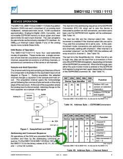
SMD1102 / 1103 / 1113
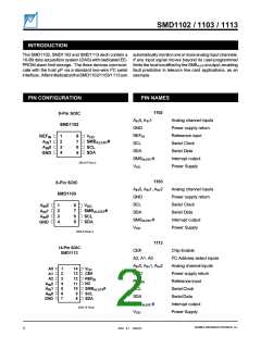
PIN DESCRIPTIONS
Serial Clock (SCL)
AIN0, AIN1, AIN2
The SCL input is used to clock data into and out of the Multiplexer input pins for channels 0, 1, and 2, respec-
device. IntheWRITEmodedatamustremainstablewhile tively. AIN2 is only available on the SMD1103 and
SCL is HIGH. In the READ mode data is clocked out on SMD1113. Thesepinsmaybeleftunconnectediftheyare
the falling edge of SCL.
not used. However, the Alert Regions must be set
accordingly (see the section "Alert Conditions").
Serial Data (SDA)
A0, A1, A2
TheSDApinisabidirectionalpinusedtotransferdatainto
and out of the device. Data may change only when SCL The address inputs are only available on the SMD1113.
is LOW, except during START and STOP conditions. It is MultipleSMD1113scanbeusedonasinglebusbysetting
an open-drain output and may be wire-ORed with any different device addresses. A2 has a 50kΩ pull-up
number of open-drain or open-collector outputs.
resistor, and A1 and A0 have 50kΩ pull-down resistors.
Do not set the address to all zeroes because it would
cause a conflict with the SMB Alert Response.
SMBALERT
#
This interrupt output pin signals the host when an out-of-
limit condition is detected by one of the EEPROM limit
CE#
registers. The SMBALERT open-drain output is active low. Chip Enable/disable input must be held low to enable I2C
communications. It has a 50kΩ pull-down resistor and is
only available on the SMD1113.
REFIN
Voltage reference input for 10-Bit A/D converter. This
VDD
signal is only on the SMD1102 and SMD1113.
Power supply input.
GND
Power supply return.
SUMMIT MICROELECTRONICS, Inc.
2033 8.1 10/04/01
4

 SUMMIT [ SUMMIT MICROELECTRONICS, INC. ]