UPSD3212C, UPSD3212CV
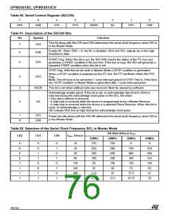
Table 50. Serial Control Register (S2CON)
7
6
5
4
3
2
1
0
CR2
ENII
STA
STO
ADDR
AA
CR1
CR0
Table 51. Description of the S2CON Bits
Bit
Symbol
Function
This bit along with Bits CR1and CR0 determines the serial clock frequency when SIO is
in the Master Mode.
7
CR2
Enable IIC. When ENI1 = 0, the IIC is disabled. SDA and SCL outputs are in the high
impedance state.
6
5
ENII
STA
2
START Flag. When this bit is set, the SIO H/W checks the status of the I C-bus and
generates a START condition if the bus free. If the bus is busy, the SIO will generate a
repeated START condition when this bit is set.
STOP Flag. With this bit set while in Master Mode a STOP condition is generated.
2
2
When a STOP condition is detected on the I C bus, the I C hardware clears the STO
Flag.
Note: This bit have to be set before 1 cycle interrupt period of STOP. That is, if this bit is
4
3
STO
set, STOP condition in Master Mode is generated after 1 cycle interrupt period.
ADDR
This bit is set when address byte was received. Must be cleared by software.
Acknowledge enable signal. If this bit is set, an acknowledge (low level to SDA) is
returned during the acknowledge clock pulse on the SCL line when:
• Own slave address is received
2
AA
• A data byte is received while the device is programmed to be a Master Receiver
• A data byte is received while the device is a selected Slave Receiver. When this bit is
reset, no acknowledge is returned.
SIO release SDA line as high during the acknowledge clock pulse.
1
0
CR1
CR0
These two bits along with the CR2 Bit determine the serial clock frequency when SIO is
in the Master Mode.
Table 52. Selection of the Serial Clock Frequency SCL in Master Mode
Bit Rate (kHz) at f
OSC
f
Divisor
CR2
CR1
CR0
OSC
12MHz
375
250
200
100
50
24MHz
750
500
400
200
100
50
36MHz
X
40MHz
X
0
0
0
0
1
1
1
1
0
0
1
1
0
0
1
1
0
1
0
1
0
1
0
1
16
24
750
600
300
150
75
833
666
333
166
83
30
60
120
240
480
960
25
12.5
6.25
25
37.5
18.75
41
12.5
20
76/152

 STMICROELECTRONICS [ ST ]