UPSD3212C, UPSD3212CV
2
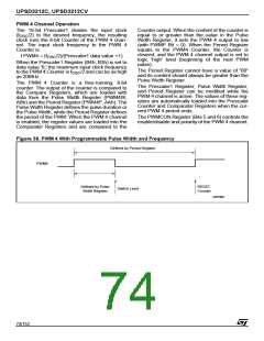
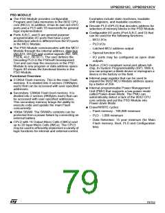
I C INTERFACE
2
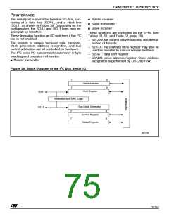
The serial port supports the twin line I C-bus, con-
sisting of a data line (SDA1), and a clock line
(SCL1) as shown in Figure 39. Depending on the
configuration, the SDA1 and SCL1 lines may re-
quire pull-up resistors.
■ Master receiver
■ Slave transmitter
■ Slave receiver
These functions are controlled by the SFRs (see
Tables 50, 51, and Table 52, page 76):
– S2CON: the control of byte handling and the op-
eration of 4 mode.
– S2STA: the contents of its register may also be
used as a vector to various service routines.
– S2DAT: data shift register.
2
These lines also function as I/O port lines if the I C
bus is not enabled.
The system is unique because data transport,
clock generation, address recognition, and bus
control arbitration are all controlled by hardware.
2
The I C serial I/O has complete autonomy in byte
handling and operates in 4 modes.
■ Master transmitter
– S2ADR: slave address register. Slave address
recognition is performed by On-Chip H/W.
2
Figure 39. Block Diagram of the I C Bus Serial I/O
7
0
0
Slave Address
7
Shift Register
SDA1
SCL1
Arbitration and Sync. Logic
Bus Clock Generator
7
7
0
0
Control Register
Status Register
AI07430
75/152

 STMICROELECTRONICS [ ST ]