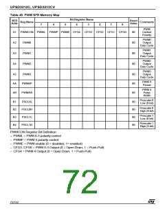
UPSD3212C, UPSD3212CV
ANALOG-TO-DIGITAL CONVERTOR (ADC)
The analog to digital (A/D) converter allows con-
version of an analog input to a corresponding 8-bit
digital value. The A/D module has four analog in-
puts, which are multiplexed into one sample and
hold. The output of the sample and hold is the in-
put into the converter, which generates the result
via successive approximation. The analog supply
voltage is connected to AVREF of ladder resis-
tance of A/D module.
matically when A/D conversion is completed,
cleared when A/D conversion is in process.
The ASCL should be loaded with a value that re-
sults in a clock rate of approximately 6MHz for the
ADC using the following formula (see Table 48,
page 69):
ADC clock input = (f
value +1)
/ 2) / (Prescaler register
OSC
Where f
is the MCU clock input frequency
OSC
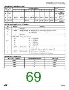
The A/D module has two registers which are the
control register ACON and A/D result register
ADAT. The register ACON, shown in Table 46 and
Table 47, page 69, controls the operation of the A/
D converter module. To use analog inputs, I/O is
selected by P1SFS register. Also an 8-bit prescal-
er ASCL divides the main system clock input down
to approximately 6MHz clock that is required for
the ADC logic. Appropriate values need to be load-
ed into the prescaler based upon the main MCU
clock frequency prior to use.
The processing of conversion starts when the
Start Bit ADST is set to '1.' After one cycle, it is
cleared by hardware. The register ADAT contains
the results of the A/D conversion. When conver-
sion is completed, the result is loaded into the
ADAT the A/D Conversion Status Bit ADSF is set
to '1.'
The conversion time for the ADC can be calculat-
ed as follows:
ADC Conversion Time = 8 clock * 8bits * (ADC
Clock) ~= 10.67usec (at 6MHz)
ADC Interrupt
The ADSF Bit in the ACON register is set to '1'
when the A/D conversion is complete. The status
bit can be driven by the MCU, or it can be config-
ured to generate a falling edge interrupt when the
conversion is complete.
The ADSF Interrupt is enabled by setting the ADS-
FINT Bit in the PCON register. Once the bit is set,
the external INT1 Interrupt is disabled and the
ADSF Interrupt takes over as INT1. INT1 must be
configured as if it is an edge interrupt input. The
INP1 pin (p3.3) is available for general I/O func-
tions, or Timer1 gate control.
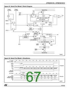
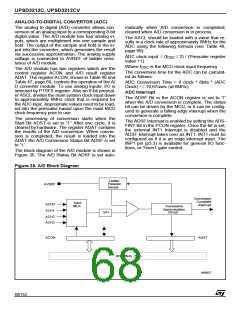
The block diagram of the A/D module is shown in
Figure 35. The A/D Status Bit ADSF is set auto-
Figure 35. A/D Block Diagram
Ladder
Resistor
AVREF
Decode
Conversion
Complete
Interrupt
Input
MUX
ACH0
ACH1
Successive
Approximation
Circuit
S/H
ACH2
ACH3
ACON
ADAT
INTERNAL BUS
AI06627
68/152

 STMICROELECTRONICS [ ST ]