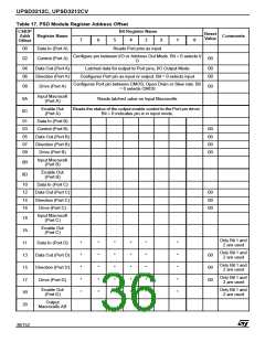
UPSD3212C, UPSD3212CV
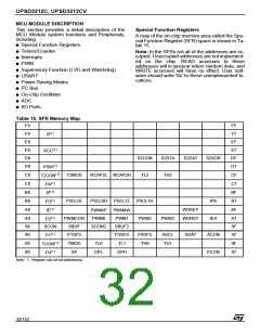
MCU MODULE DISCRIPTION
This section provides a detail description of the
MCU Module system functions and Peripherals,
including:
Special Function Registers
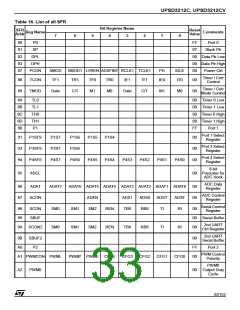
A map of the on-chip memory area called the Spe-
cial Function Register (SFR) space is shown in Ta-
ble 15.
■ Special Function Registers
■ Timers/Counter
Note: In the SFRs not all of the addresses are oc-
cupied. Unoccupied addresses are not implement-
ed on the chip. READ accesses to these
addresses will in general return random data, and
WRITE accesses will have no effect. User soft-
ware should write '0s' to these unimplemented lo-
cations.
■ Interrupts
■ PWM
■ Supervisory Function (LVD and Watchdog)
■ USART
■ Power Saving Modes
2
■ I C Bus
■ On-chip Oscillator
■ ADC
■ I/O Ports
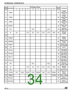
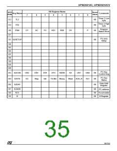
Table 15. SFR Memory Map
F8
FF
F7
EF
E7
(1)
F0
E8
E0
D8
D0
C8
C0
B8
B0
A8
A0
98
90
88
80
B
(1)
(1)
ACC
S2CON
TL2
S2STA
TH2
S2DAT
S2ADR
DF
D7
CF
C7
BF
B7
AF
A7
9F
97
PSW
(1)
T2MOD
PSCL0L
RCAP2L RCAP2H
T2CON
(1)
P4
(1)
IP
(1)
PSCL0H
PSCL1L PSCL1H
PWM4W
IPA
P3
(1)
WDKEY
WDRST
IE
PWM4P
PWM0
(1)
PWMCON
SBUF
PWM1
SBUF2
P3SFS
TL1
PWM2
PWM3
IEA
P2
SCON
SCON2
(1)
P1SFS
TMOD
SP
P4SFS
TH0
ASCL
TH1
ADAT
ACON
P1
(1)
TL0
8F
87
TCON
(1)
DPL
DPH
PCON
P0
Note: 1. Register can be bit addressing
32/152

 STMICROELECTRONICS [ ST ]