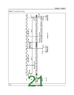
TS5070 - TS5071
100%electricaltestingat TA =25°C. All otherlimits
are assured by correlation with other production
tests and/or product design and characterisation.
All signalsreferencedto GND.Typicalsspecifiedat
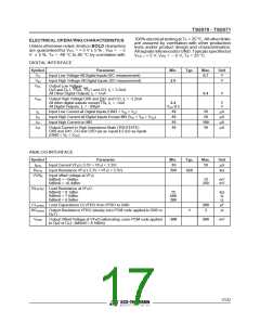
ELECTRICAL OPERATING CHARACTERISTICS
Unless otherwise noted, limits in BOLD characters
±
are guaranteedfor VCC = + 5 V 5 % ; VSS = – 5
V ± 5 %. TA = -40 °C to 85 °C by correlation with
VCC = + 5 V, VSS = − 5 V, TA = 25 °C.
DIGITAL INTERFACE
Symbol
VIL
Parameter
Min.
2.0
Typ.
Max.
0.7
Unit
V
Input Low Voltage All Digital Inputs (DC measurement)
Input High Voltage All Digital Inputs (DC measurement)
VIH
V
VOL
Output Low Voltage
DX0 and DX1, TSX0, TSX1 and CO, IL = 3.2mA
All Other Digital Outputs, IL = 1mA
0.4
V
VOH
Output High Voltage DX0 and DX1 and CO, IL = -3.2mA
All other digital outputs except TSX, IL = -1mA
All Digital Outputs, IL = -100µA
2.4
VCC-0.5
V
V
IIL
IIH
Input Low Current all Digital Inputs (GND < VIN < VIL)
-10
-10
-10
-10
10
10
A
µ
Input High Current all Digital Inputs Except MR (VIH < VIN < VCC
)
µA
µA
µA
IIH
Input High Current on MR
100
10
IOZ
Output Current in High Impedance State (TRI-STATE)
DX0 and DX1, CO and CI/O (as an input) IL5-IL0 as inputs
(GND < VO < VCC
)
ANALOG INTERFACE
Symbol
Parameter
Min.
-10
Typ.
620
Max.
10
Unit
µA
IVFXI
RVFXI
VOSX
Input Current VFXI (-3.3V < VFXI < 3.3V)
Input Resistance VFXI (-3.3V < VFXI < 3.3V)
390
kΩ
Input offset voltage at VFXI
0dBm0 = -19dBm
0dBm0 = +6.4dBm
10
200
mV
mV
RLVFRO Load Resistance at VFRO
0dBm0 = 8.1dBm
15
k
Ω
0dBm0 = 7.6dBm
0dBm0 = 6.9dBm
600
300
Ω
Ω
pF
Ω
CLVFRO Load Capacitance CLVFRO from VFRO to GND
200
3
ROVFRO Output Resistance VFRO (steady zero PCM code applied to DR0 or
DR1)
1
VOSR
Output Offset Voltage at VFRO (alternating ±zero PCM code applied
-200
200
mV
to DR0 or DR1, 0dBm0 = 8.1dBm)
17/32

 STMICROELECTRONICS [ ST ]