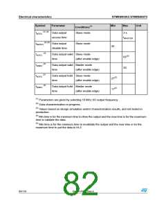
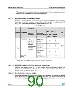
Electrical characteristics
STM8S903K3 STM8S903F3
Symbol Parameter
Conditions
Min
Typ Max
Unit
VDD =4.5 to 5.5 V
1
-
-
6
VAIN
Conversion voltage range(1)
VSS
VDD
V
V
VBGREF Internal bandgap reference
voltage
VDD =2.95 to 5.5 V 1.19 1.22 1.25
CADC
Internal sample and hold
capacitor
-
3
-
pF
µs
(1)
tS
Minimum sampling time
fADC = 4 MHz
fADC = 6 MHz
-
-
-
0.75
0.5
-
-
-
tSTAB
Wake-up time from standby
µs
µs
7
tCONV
Minimum total conversion
time (including sampling time,
10-bit resolution)
fADC = 4 MHz
fADC = 6 MHz
3.5
2.33
14
µs
1/fADC
(1) During the sample time the input capacitance CAIN (3 pF max) can be charged/discharged
by the external source. The internal resistance of the analog source must allow the
capacitance to reach its final voltage level within tS. After the end of the sample time tS,
changes of the analog input voltage have no effect on the conversion result. Values for the
sample clock tS depend on programming.
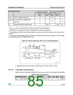
Table 48: ADC accuracy with RAIN < 10 kΩ , VDD= 5 V
Symbol Parameter
Conditions
Typ
1.6
Max(1) Unit
|ET|
|EO|
|EG|
|ED|
Total unadjusted error(2)
fADC = 2 MHz
fADC = 4 MHz
fADC = 6 MHz
fADC = 2 MHz
fADC = 4 MHz
fADC = 6 MHz
fADC = 2 MHz
fADC = 4 MHz
fADC = 6 MHz
fADC = 2 MHz
fADC = 4 MHz
3.5
4
LSB
2.2
2.4
1.1
1.5
1.8
1.5
2.1
2.2
0.7
0.7
4.5
2.5
3
Offset error(2)
3
Gain error(2)
3
3
4
Differential linearity error(2)
1.5
1.5
86/116
DocID15590 Rev 8

 STMICROELECTRONICS [ ST ]