Electrical characteristics
STM8S903K3 STM8S903F3
(1)Data obtained with HSI clock configuration, after applying HW recommendations described
in AN2860 (EMC guidelines for STM8S microcontrollers).
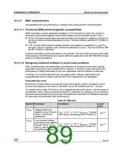
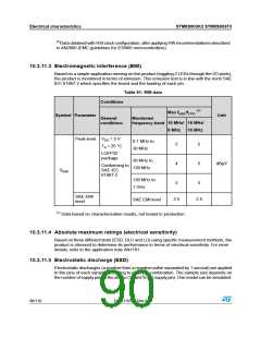
10.3.11.3 Electromagnetic interference (EMI)
Based on a simple application running on the product (toggling 2 LEDs through the I/O ports),
the product is monitored in terms of emission. This emission test is in line with the norm SAE
IEC 61967-2 which specifies the board and the loading of each pin.
Table 51: EMI data
Conditions
(1)
Max fHSE/fCPU
Symbol Parameter
Unit
General
Monitored
16 MHz/ 16 MHz/
conditions
frequency band
8 MHz
16 MHz
Peak level VDD = 5 V
TA = 25 °C
0.1 MHz to
30 MHz
5
5
LQFP32
package
30 MHz to
130 MHz
4
5
dBμV
Conforming to
SAE IEC
61967-2
SEMI
130 MHz to
1 GHz
5
5
SAE EMI
level
2.5
2.5
SAE EMI level
(1) Data based on characterisation results, not tested in production.
10.3.11.4 Absolute maximum ratings (electrical sensitivity)
Based on three different tests (ESD, DLU and LU) using specific measurement methods, the
product is stressed to determine its performance in terms of electrical sensitivity. For more
details, refer to the application note AN1181.
10.3.11.5 Electrostatic discharge (ESD)
Electrostatic discharges (a positive then a negative pulse separated by 1 second) are applied
to the pins of each sample according to each pin combination. The sample size depends on
the number of supply pins in the device (3 parts*(n+1) supply pin). One model can be simulated:
90/116
DocID15590 Rev 8

 STMICROELECTRONICS [ ST ]