STM8S903K3 STM8S903F3
Electrical characteristics
10.3.11 EMC characteristics
Susceptibility tests are performed on a sample basis during product characterization.
10.3.11.1 Functional EMS (electromagnetic susceptibility)
While executing a simple application (toggling 2 LEDs through I/O ports), the product is
stressed by two electromagnetic events until a failure occurs (indicated by the LEDs).
FESD: Functional electrostatic discharge (positive and negative) is applied on all pins of
the device until a functional disturbance occurs. This test conforms with the IEC 61000-4-2
standard.
•
FTB: A burst of fast transient voltage (positive and negative) is applied to VDD and VSS
through a 100 pF capacitor, until a functional disturbance occurs. This test conforms with
the IEC 61000-4-4 standard.
•
A device reset allows normal operations to be resumed. The test results are given in the table
below based on the EMS levels and classes defined in application note AN1709 (EMC design
guide for STMicrocontrollers).
10.3.11.2 Designing hardened software to avoid noise problems
EMC characterization and optimization are performed at component level with a typical
application environment and simplified MCU software. It should be noted that good EMC
performance is highly dependent on the user application and the software in particular.
Therefore it is recommended that the user applies EMC software optimization and
prequalification tests in relation with the EMC level requested for his application.
Prequalification trials
Most of the common failures (unexpected reset and program counter corruption) can be
recovered by applying a low state on the NRST pin or the oscillator pins for 1 second.
To complete these trials, ESD stress can be applied directly on the device, over the range of
specification values. When unexpected behavior is detected, the software can be hardened
to prevent unrecoverable errors occurring. See application note AN1015 (Software techniques
for improving microcontroller EMC performance).
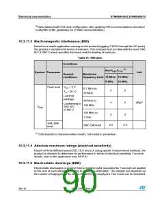
Table 50: EMS data
Symbol Parameter
Conditions
Level/
class
VFESD Voltage limits to be
applied on any I/O pin to
induce a functional
2/B (1)
VDD = 3.3 V, TA = 25 °C, fMASTER = 16 MHz
(HSI clock), conforming to IEC 61000-4-2
disturbance
VEFTB
Fast transient voltage
burst limits to be applied
through 100 pF on VDD
and VSS pins to induce a
functional disturbance
4/A (1)
VDD= 3.3 V, TA = 25 °C ,fMASTER = 16 MHz
(HSI clock),conforming to IEC 61000-4-4
DocID15590 Rev 8
89/116

 STMICROELECTRONICS [ ST ]