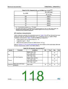
Electrical characteristics
STM32F405xx, STM32F407xx
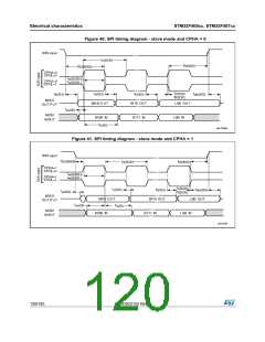
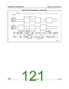
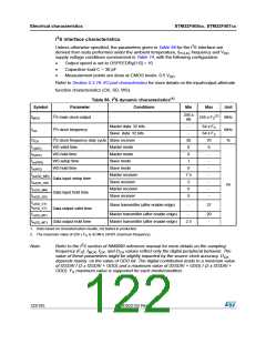
I2S interface characteristics
2
Unless otherwise specified, the parameters given in Table 56 for the i S interface are
derived from tests performed under the ambient temperature, f
frequency and V
PCLKx
DD
supply voltage conditions summarized in Table 14, with the following configuration:
•
•
•
Output speed is set to OSPEEDRy[1:0] = 10
Capacitive load C = 30 pF
Measurement points are done at CMOS levels: 0.5 V
DD
Refer to Section 5.3.16: I/O port characteristics for more details on the input/output alternate
function characteristics (CK, SD, WS).
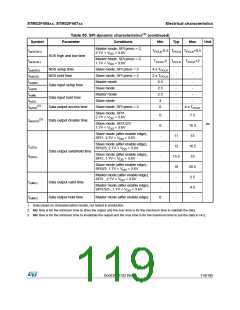
2
(1)
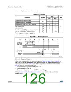
Table 56. I S dynamic characteristics
Symbol
Parameter
Conditions
Min
Max
Unit
256 x
8K
(2)
fMCK
I2S main clock output
-
256 x FS
MHz
Master data: 32 bits
Slave data: 32 bits
-
-
64 x FS
fCK
I2S clock frequency
MHz
%
64 x FS
DCK
I2S clock frequency duty cycle Slave receiver
30
0
70
6
-
tv(WS)
WS valid time
WS hold time
WS setup time
WS hold time
Master mode
Master mode
Slave mode
th(WS)
0
tsu(WS)
1
-
th(WS)
Slave mode
0
-
tsu(SD_MR)
tsu(SD_SR)
th(SD_MR)
th(SD_SR)
Master receiver
Slave receiver
Master receiver
Slave receiver
7.5
2
-
Data input setup time
Data input hold time
-
ns
0
-
0
-
tv(SD_ST)
th(SD_ST)
Slave transmitter (after enable edge)
-
27
Data output valid time
tv(SD_MT)
Master transmitter (after enable edge)
Master transmitter (after enable edge)
-
20
-
th(SD_MT) Data output hold time
2.5
1. Data based on characterization results, not tested in production.
2. The maximum value of 256 x FS is 42 MHz (APB1 maximum frequency).
2
Note:
Refer to the I S section of RM0090 reference manual for more details on the sampling
frequency (F ). f
, f , and D values reflect only the digital peripheral behavior. The
S
MCK CK
CK
value of these parameters might be slightly impacted by the source clock accuracy. D
CK
depends mainly on the value of ODD bit. The digital contribution leads to a minimum value
of I2SDIV / (2 x I2SDIV + ODD) and a maximum value of (I2SDIV + ODD) / (2 x I2SDIV +
ODD). F maximum value is supported for each mode/condition.
S
122/185
DocID022152 Rev 4

 STMICROELECTRONICS [ ST ]