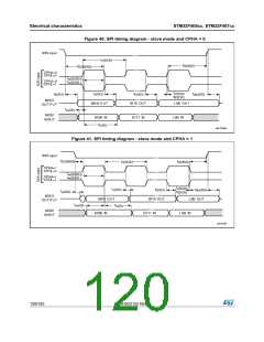
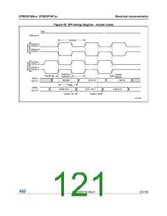
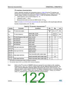
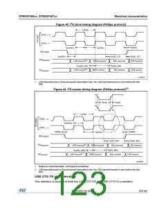
Electrical characteristics
Symbol
STM32F405xx, STM32F407xx
Table 57. USB OTG FS startup time
Parameter
Max
Unit
(1)
tSTARTUP
USB OTG FS transceiver startup time
1
µs
1. Guaranteed by design, not tested in production.
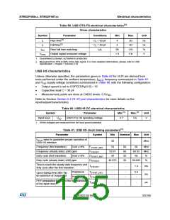
Table 58. USB OTG FS DC electrical characteristics
Symbol
Parameter
Conditions
Min.(1) Typ. Max.(1) Unit
USB OTG FS operating
voltage
VDD
3.0(2)
0.2
-
-
-
-
3.6
-
V
I(USB_FS_DP/DM,
USB_HS_DP/DM)
(3)
VDI
Differential input sensitivity
Input
levels
Differential common mode
range
(3)
VCM
Includes VDI range
0.8
2.5
2.0
V
Single ended receiver
threshold
(3)
VSE
1.3
VOL Static output level low
VOH Static output level high
RL of 1.5 kΩ to 3.6 V(4)
-
-
-
0.3
3.6
Output
levels
V
(4)
RL of 15 kΩ to VSS
2.8
PA11, PA12, PB14, PB15
(USB_FS_DP/DM,
17
21
24
USB_HS_DP/DM)
RPD
VIN = VDD
PA9, PB13
(OTG_FS_VBUS,
OTG_HS_VBUS)
0.65
1.5
1.1
1.8
2.0
2.1
kΩ
PA12, PB15 (USB_FS_DP,
USB_HS_DP)
VIN = VSS
RPU
PA9, PB13
(OTG_FS_VBUS,
OTG_HS_VBUS)
VIN = VSS
0.25 0.37 0.55
1. All the voltages are measured from the local ground potential.
2. The STM32F405xx and STM32F407xx USB OTG FS functionality is ensured down to 2.7 V but not the full
USB OTG FS electrical characteristics which are degraded in the 2.7-to-3.0 V VDD voltage range.
3. Guaranteed by design, not tested in production.
RL is the load connected on the USB OTG FS drivers
4.
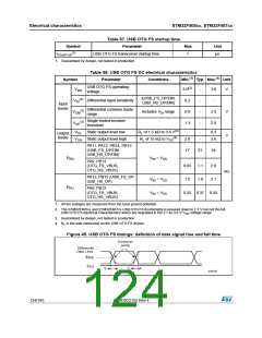
Figure 45. USB OTG FS timings: definition of data signal rise and fall time
Crossover
points
Differential
Data Lines
V
CR S
V
SS
t
t
r
f
ai14137
124/185
DocID022152 Rev 4

 STMICROELECTRONICS [ ST ]